Exposure apparatus including micro mirror array and exposure method using the same

a technology of micro-mirror array and exposure apparatus, which is applied in the field of photolithography process, can solve the problems of limited aperture shape, high probability, and no optimal match of available apertures

Inactive Publication Date: 2006-06-13
SAMSUNG ELECTRONICS CO LTD
View PDF7 Cites 227 Cited by
  • Summary
  • Abstract
  • Description
  • Claims
  • Application Information

AI Technical Summary

Benefits of technology

[0017]One object of the present invention is to an exposure method of apparatus which can form a pattern having a high degree of resolution and optimum depth of focus (DOF) on a semiconductor wafer. Another object of the present invention is to provide an exposure method and apparatus which can form a pattern in a relatively short amount of time, i.e., which are characterized by providing a short exposure time.

Problems solved by technology

First, the shapes of the available apertures are limited.
That is, only several types of apertures are available and thus, there is a high probability that none of the available apertures is an optimal match for the pattern of the selected photomask.
Accordingly, in most cases, it is difficult to precisely transcribe the pattern of a photomask and form a pattern having the highest resolution and optimum DOF on a wafer using a conventional exposure apparatus and method.
Secondly, the conventional exposure apparatus is inconvenient in that the aperture must often be exchanged during the process of manufacturing a semiconductor device.
The operation of the exposure apparatus must be temporarily discontinued while the apertures are being exchanged, thereby increasing the total time of the exposure process and consequently lowering the productivity of the manufacturing process.
Accordingly, the conventional exposure process is not marked by energy efficiency meaning that the exposure time must be long to satisfactorily complete an exposure process.
Therefore, the overall manufacturing process using the conventional exposure method and apparatus also takes a long time to complete.

Method used


Image

  • Exposure apparatus including micro mirror array and exposure method using the same
  • Exposure apparatus including micro mirror array and exposure method using the same
  • Exposure apparatus including micro mirror array and exposure method using the same

Examples


Embodiment Construction

[0033]The present invention will now be described more fully with reference to the accompanying drawings. Also, it should be noted that like reference numerals designate like elements throughout the drawings.

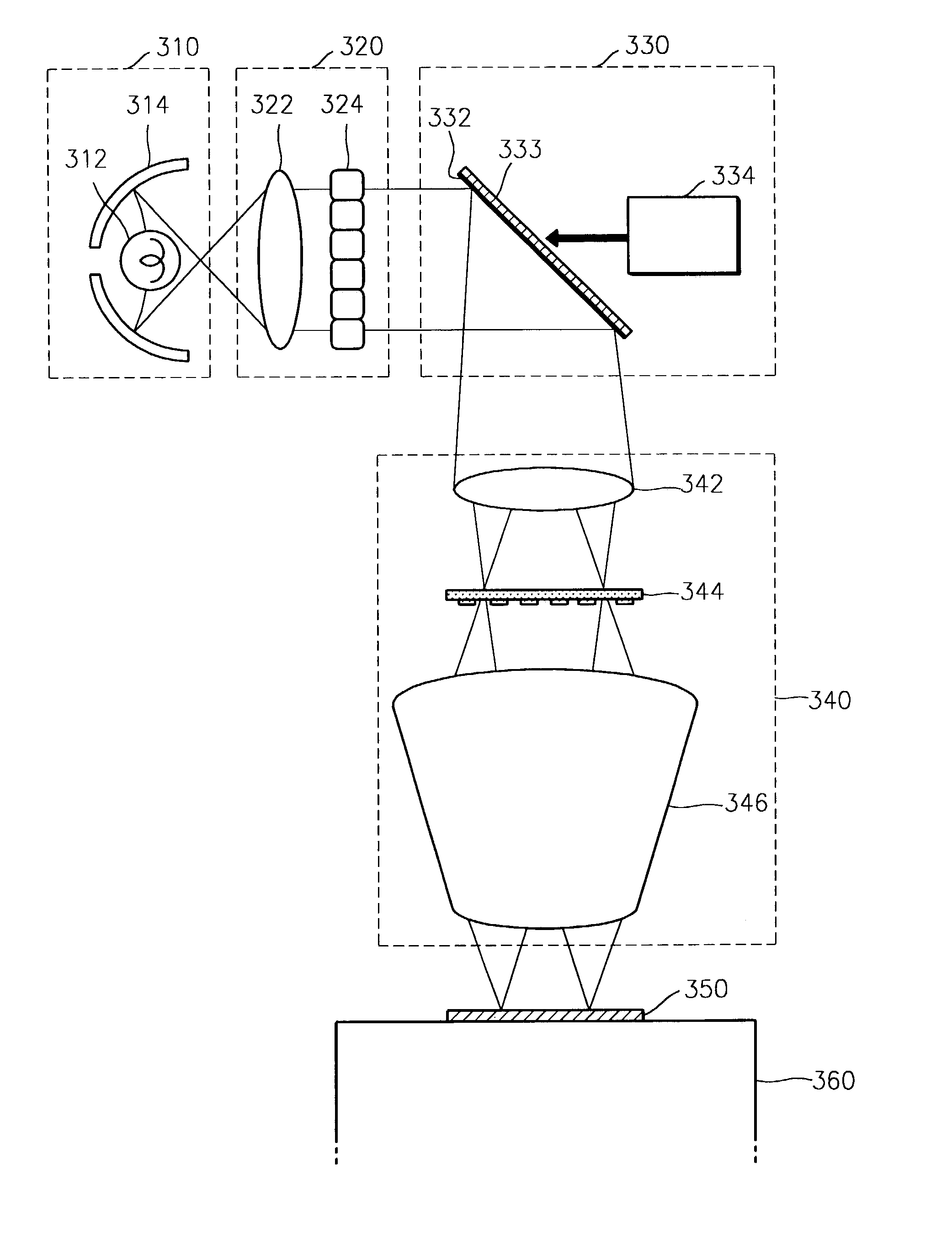
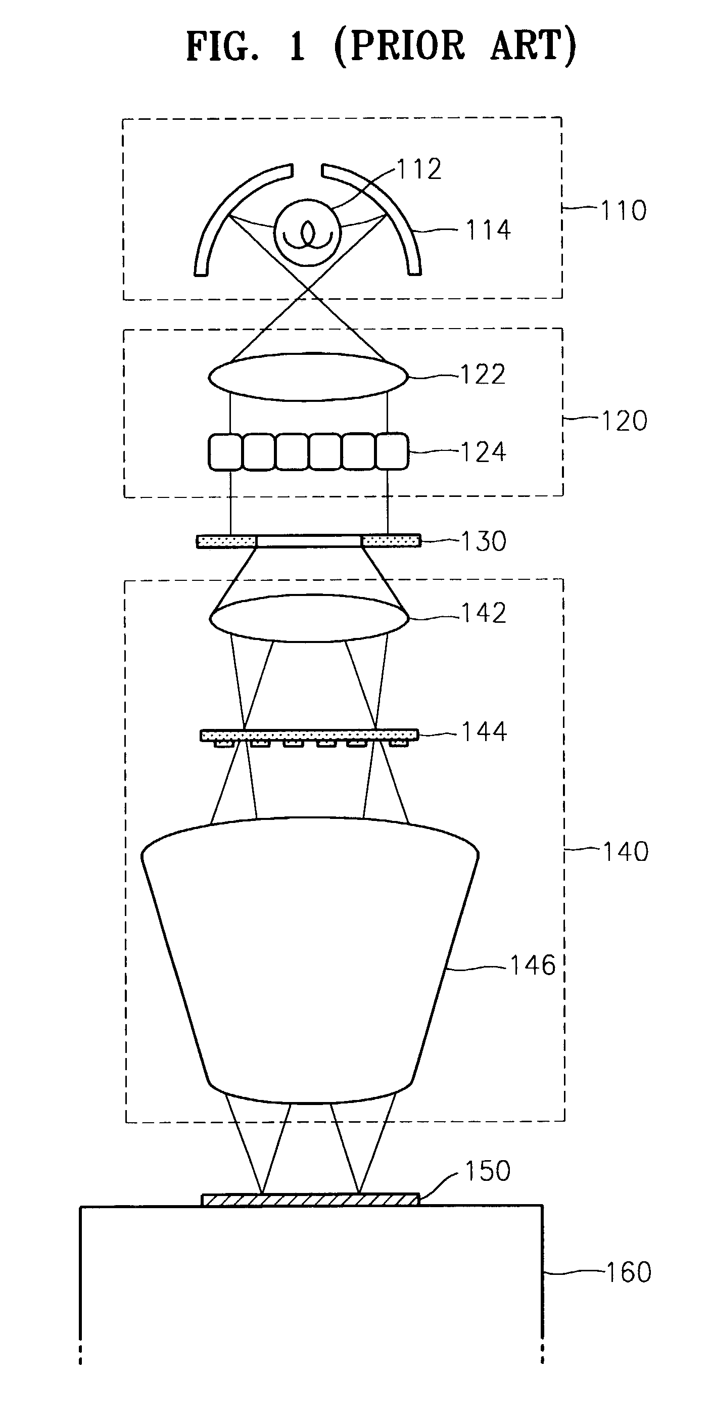
[0034]Referring first to FIG. 3, the projection-type of exposure apparatus according to the present invention includes a light source unit 310, an optical lens unit 320, a pattern transfer unit 340, and a reflecting mirror unit 330 interposed between the optical lens unit 320 and the pattern transfer unit 340 with respect to the optical axis of the apparatus. The reflecting mirror unit 330 reflects light at a desired angle from light source unit 310 to the pattern transfer unit 340. Similar to the conventional exposure apparatus shown FIG. 1, the light source unit 310 includes a light source 312 and oval mirrors 314, the optical lens unit 320 includes a collecting lens 322 and a fly's eye lens 324, and the pattern transfer unit 340 includes a photomask 344 and a projecting lens ...


PUM

PropertyMeasurementUnit
anglesaaaaaaaaaa
angles of inclinationaaaaaaaaaa
optical axisaaaaaaaaaa

Abstract

An exposure method and apparatus for use in exposing a photoresist on a semiconductor wafer do not employ an aperture for shaping the exposure light. The exposure apparatus includes a light source unit, a reflecting mirror unit having a micro mirror array (MMA) and a control unit that controls the MMA, and a pattern transfer unit that transfers the pattern of a photomask onto the photoresist. The angles of inclination of the respective mirrors of the MMA are adjusted to reflect incident light in a manner that shapes the incident light. Accordingly, it is possible to form a pattern having the highest degree of resolution and optimum depth of focus (DOF) in the shortest amount of processing time.

Description

BACKGROUND OF THE INVENTION[0001]1. Field of the Invention[0002]The present invention relates to the photolithography process used in the manufacturing of semiconductor devices. More particularly, the present invention relates to a method of and an apparatus for exposing a semiconductor wafer to transcribe a pattern onto the wafer.[0003]2. Description of the Related Art[0004]Photolithography is one of the major processes of manufacturing a semiconductor device as it is indispensable to the overall process of forming a particular circuit on a wafer. In general, photolithography includes a series of individual processes such as a process of coating a substrate with a photoresist, an exposure process in which the photoresist is exposed to light of a given wavelength, and a process of developing the exposed photoresist. In the exposure process, light is directed through a mask having a particular pattern to transcribe the pattern onto the wafer.[0005]The higher the degree of integration...

Claims


Application Information

Patent Timeline
Patent Type & Authority Patents(United States)
IPC IPC(8): G03B27/54G03B27/42G03B27/62H01L21/027G03F7/20
CPCG03F7/70116G03B27/54H01L21/027
Inventor ZINN, SHUN YONGKIM, YONG HOONYANG, SEUNG HUNE
Owner SAMSUNG ELECTRONICS CO LTD
Why Eureka
Try Eureka