JFET controlled schottky barrier diode

a schottky diode and control technology, applied in the direction of transistors, electrical apparatus, semiconductor devices, etc., can solve the problems of unfavorable current flow through the schottky diode, leakage current, affecting the efficiency of the voltage converter at higher voltages,

Active Publication Date: 2006-06-20
MICREL
View PDF4 Cites 101 Cited by
  • Summary
  • Abstract
  • Description
  • Claims
  • Application Information

AI Technical Summary

Benefits of technology

[0007]According to one embodiment of the present invention, a JFET controlled Schottky barrier diode includes a p-type diffusion region integrated into the cathode of the Schottky diode to form an integrated JFET where the integrated JFET provides on-off control of the Schottky barrier diode. The p-type diffusion region encloses a portion of the forward current path of the Schottky barrier diode

Problems solved by technology

However, when the voltage converter is not being used, the DC current path remains which results in undesirable current flow through the Schottky diode to the output load.
When the output boost voltage at the cathode is about the same as the supply v

Method used


Image

  • JFET controlled schottky barrier diode
  • JFET controlled schottky barrier diode
  • JFET controlled schottky barrier diode

Examples


Embodiment Construction

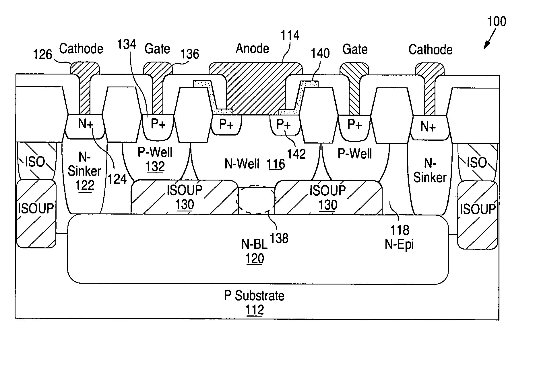
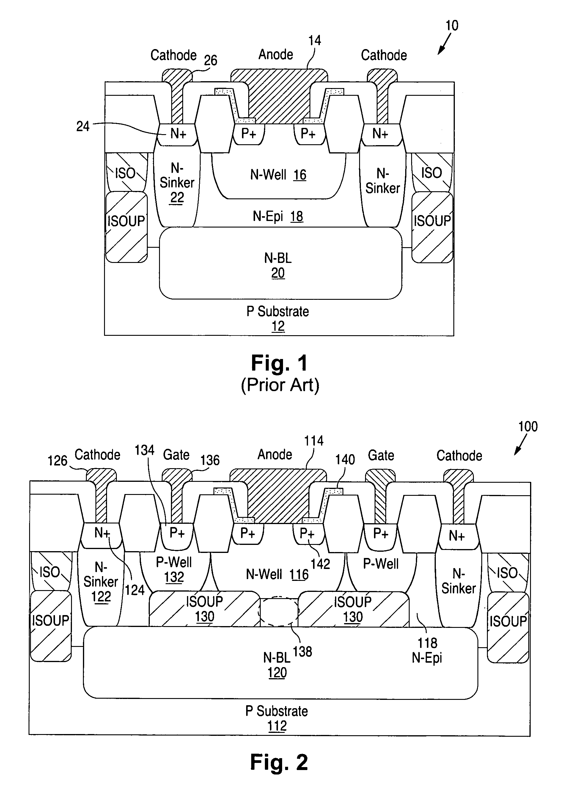
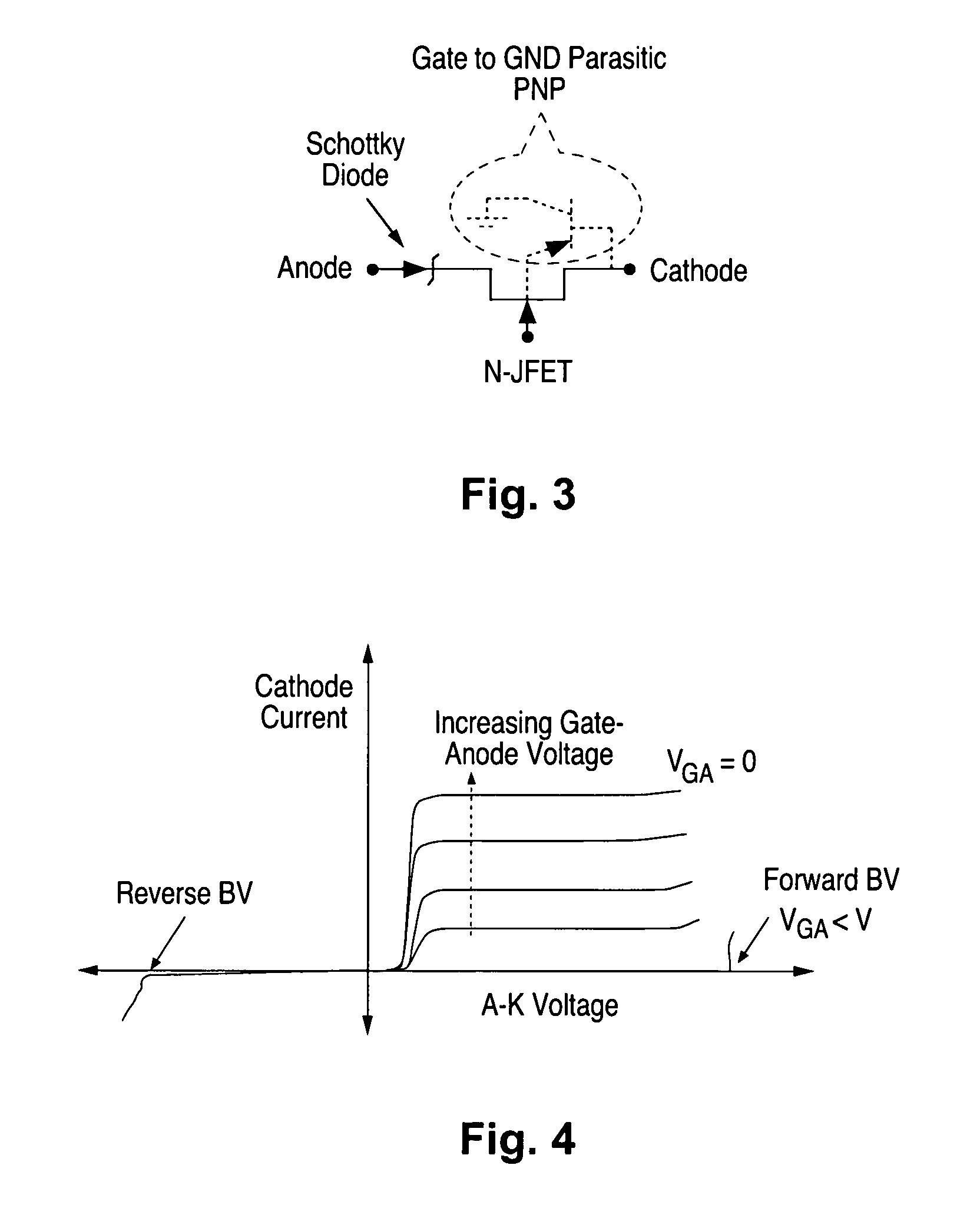
[0016]In accordance with the principles of the present invention, a Schottky barrier diode includes an integrated junction field-effect transistor (JFET) for providing on-off control of the Schottky barrier diode. The Schottky barrier diode thus formed is referred herein as a “JFET Controlled Schottky Diode.” Specifically, a p-type diffusion region is integrated into the cathode of the Schottky diode to realize a reverse biased p-n junction where the p-n junction operates to pinch off the forward current of the Schottky diode using JFET action. By applying a reverse biased potential to the integrated JEFT with respect to the anode, on-off control over the Schottky diode forward current is realized.

[0017]FIG. 2 is a cross-sectional view of a JFET controlled Schottky diode according to one embodiment of the present invention. The equivalent circuit of the JFET controlled Schottky diode is shown in FIG. 3. Referring to FIG. 2, JFET controlled Schottky diode 100 (hereinafter “Schottky d...


PUM


Abstract

A JFET controlled Schottky barrier diode includes a p-type diffusion region integrated into the cathode of the Schottky diode to form an integrated JFET where the integrated JFET provides on-off control of the Schottky barrier diode. The p-type diffusion region encloses a portion of the forward current path of the Schottky barrier diode where the p-type diffusion region forms the gate of the JFET and the enclosed portion of the forward current path forms the channel region of the JFET. By applying a reverse biased potential to the gate of the JEFT with respect to the anode of the Schottky diode, the forward current of the Schottky diode can be pinched off, thereby providing on-off control over the Schottky diode forward current.

Description

FIELD OF THE INVENTION[0001]The invention relates to a Schottky barrier diode with turn-off control and, in particular, to a Schottky barrier diode incorporating a JEFT for controlling the on-off state of the Schottky diode.DESCRIPTION OF THE RELATED ART[0002]A Schottky barrier diode (or a “Schottky diode”) is formed by a metal-semiconductor junction. A barrier metal is deposited on the surface of a lightly doped N-type or P-type semiconductor to form the diode junction. For example, aluminum can be deposited on the surface of a lightly doped N-type semiconductor to form a Schottky barrier diode. The barrier metal contacting the N-type semiconductor forms the anode of the Schottky diode. The cathode of the Schottky diode is formed by an N+ region in electrical contact with the lightly doped semiconductor region. A Schottky barrier diode is characterized by a low forward voltage as compared to traditional p-n junction diodes. Conventional Schottky diodes conduct in forward mode whene...

Claims


Application Information

Patent Timeline
IPC IPC(8): H01L27/095H01L29/47H01L29/812H01L31/07H01L31/108
CPCH01L27/0727H01L27/095H01L29/8083H01L29/0843H01L27/098
Inventor MALLIKARJUNASWAMY, SHEKAR
Owner MICREL
Why Eureka
Try Eureka