Electron source structure covered with resistance film

a technology of resistance film and electron source, which is applied in the manufacture of electrode systems, discharge tube main electrodes, electric discharge tubes/lamps, etc., can solve the problems of increasing the total power consumption of the entire electronic device, increasing the total power consumption of the electronic device, and not being able to prevent the substrate from being charged in sufficient degree. , to achieve the effect of increasing the thickness

Inactive Publication Date: 2006-06-20
CANON KK
View PDF32 Cites 20 Cited by
  • Summary
  • Abstract
  • Description
  • Claims
  • Application Information

AI Technical Summary

Benefits of technology

[0007]The present invention has been made with a view to solve the above-mentioned problems and an object of the present invention is therefore to provide a novel structure of a resistance film formed on an insulating substrate surface and a manufacturing method therefor.
[0008]According to an aspect of the present invention, there is provided an electronic device such as an electron source, including: an insulating substrate; a conductor; and a resistance film connected with the conductor, the conductor and the resistance film being formed on the insulating substrate,
[0009]in which the resistance film has a larger thickness in a connection region with the conductor than a thickness in portions other than the connection region.
[0010]Also, according to another aspect of the present invention, there is provided an electron source, including: an insulating substrate; an electron-emitting region; a conductor electrically connected with the electron-emitting region; and a resistance film connected with the conductor, the electron-emitting region, the conductor, and the resistance film being formed on the insulating substrate, in which the resistance film has a larger thickness in a connection region with the conductor than a thickness in portions other than the connection region.
[0011]Also, according to another aspect of the present invention, there is provided a manufacturing method for an electronic device substrate, including: forming a substrate whose surface has an insulating region and an electroconductive region; performing surface treatment on the substrate for reducing a contact angle in the electroconductive region to less than 80°; and forming a resistance film to extend region of the substrate on which the surface treatment is performed.
[0012]Further, as a preferred embodiment of the present invention, there is provided a manufacturing 0method for an electronic device, specifically, an electron source, including: forming a plurality of electron-emitting devices and a plurality of porous wirings for driving the plurality of electron-emitting devices on a part of an insulating substrate; and applying an solution that contains electorconductive material or precursor onto a surface of the insulating substrate having the plurality of electron-emitting devices and the plurality of porous wirings formed thereon and drying the solution that contains electorconductive material or precursor to thereby form a resistance film extending over the plurality of porous wirings and the surface of the insulating substrate, in which the solution that contains electorconductive material or precursor is applied in an amount not smaller than a saturation point of solution absorption of the plurality of porous wirings.

Problems solved by technology

In such cases, there arises a problem in that the surface of the insulating substrate is charged while the electronic device operates, so that operation conditions of the electronic device may be altered or become unstable.
Meanwhile, a current flowing through the resistance film causes an increase in total power consumption of the entire electronic device.
In contrast, when placing an emphasis on a reduction in power consumption, the substrate is not sufficiently prevented from being charged.
As a result, an undesirable leak current is increased as well as an electron emission amount is decreased.
Also, the above problem is not caused exclusively in the surface conduction electron-emitting devices, i.e., electron-emitting devices other than the surface conduction electron-emitting devices encounter the problem in some cases.

Method used


Image

  • Electron source structure covered with resistance film
  • Electron source structure covered with resistance film
  • Electron source structure covered with resistance film

Examples


embodiment 1

[0028]Hereinafter, description will be made of the present invention by way of more specific examples.

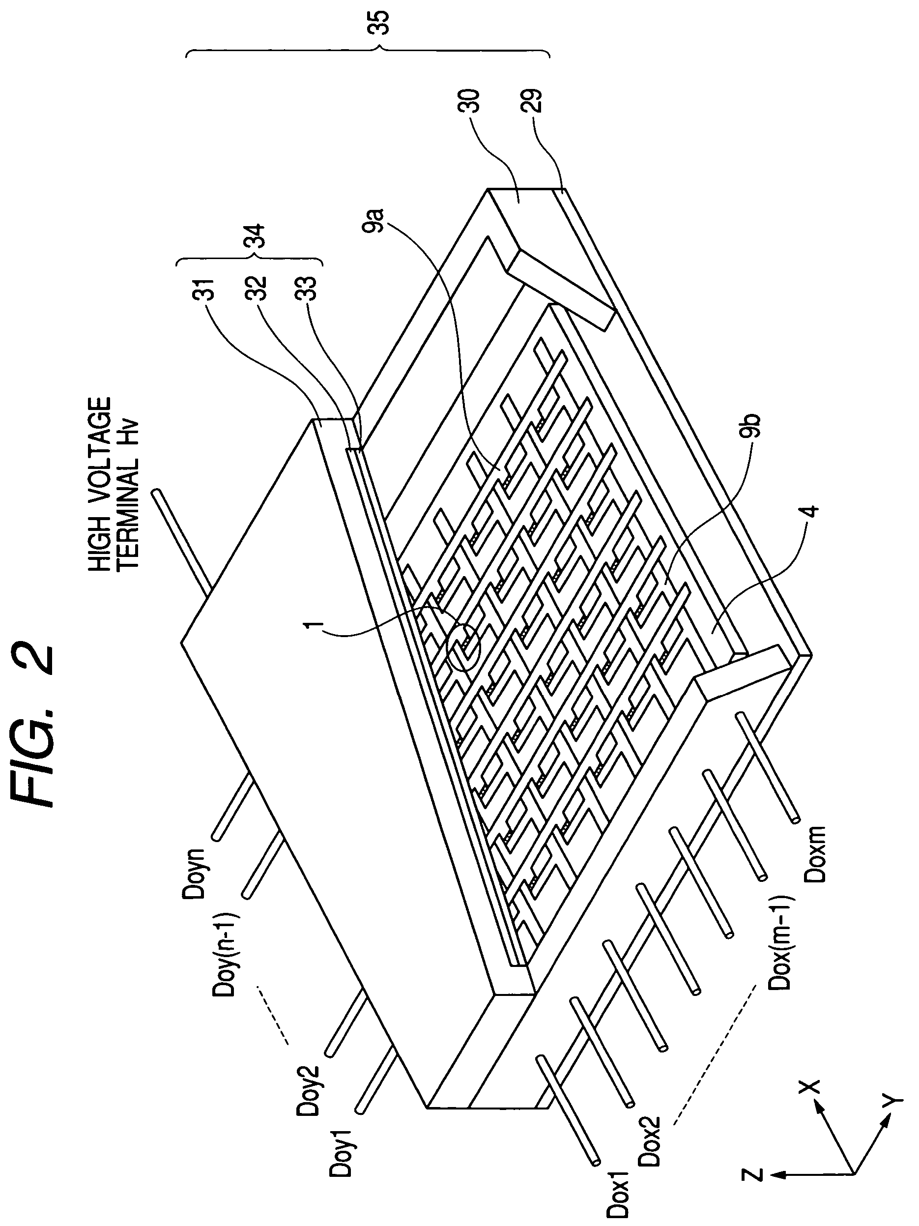
[0029]A plurality of electron-emitting devices each having the same construction as that of FIG. 1 are arranged, as schematically shown in FIG. 2, on a base to constitute a display device. An electron source (denoted by reference numeral 4 in FIG. 2) having plural electron-emitting devices arranged in matrix is manufactured through procedures described below.

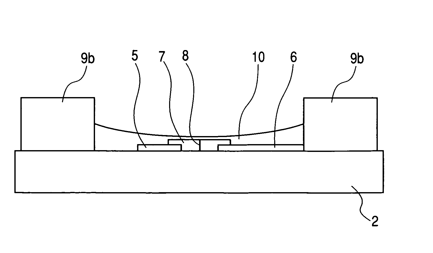
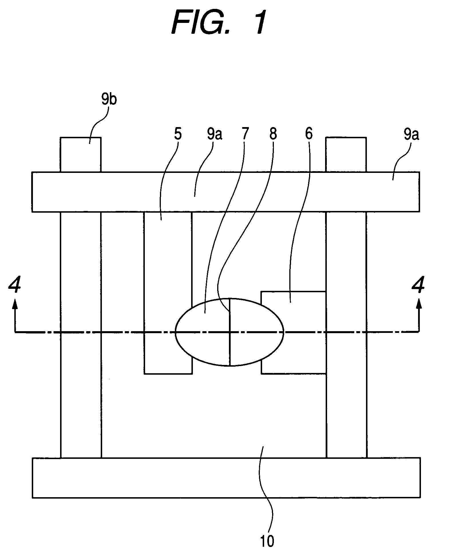
[0030]In FIG. 1, reference numeral 7 denotes an electroconductive thin film, and reference numerals 5 and 6 denote device electrodes. Reference symbols 9a and 9b denote X-direction wiring and Y-direction wiring, respectively.

[0031]It should be noted here that an insulating layer is formed in actuality between the Y-direction wiring and the X-direction wiring, but for the ease of understanding the construction, those components are partially omitted in the drawing.

[0032]Next, description is given of a specific manufacturing metho...

embodiment 2

[0078]In Embodiment 2, an electroconductive paste containing silver is used for forming Y-direction wiring, and the number of organic polymer binder compositions is set larger than that of Embodiment 1. This wiring becomes porous after baking and then absorbs low viscosity liquid.

[0079]With such porous properties, when liquid is absorbed until saturation, affinity for the liquid becomes extremely high and thus droplets are not formed on the surface, whereby a surface having the contact angle of substantially 0° is formed.

[0080]In this embodiment, upon coating of the resistance film 10, a concentration of the solution is reduced to half as compared to Embodiment 1, but instead in order that the coating amount per unit area becomes double, the head movement velocity is halved to allow the coating amount to be larger than that the saturation point with respect to the absorbing amount of the wiring.

[0081]Specific conditions are as follows.

[0082]The resistance film 10 is obtained by disp...

embodiment 3

[0093]The same assembly procedures as those in Embodiment 1 are generally performed in Embodiment 3.

[0094]Also, the coating conditions of the resistance film 10 are the same as those of Embodiment 1.

[0095]Before the formation of the resistance film 10, the insulating surface is subjected to hydrophobization processing using tetraethoxyorganosilane (TEOS).

[0096]To be specific, TEOS and the substrate are hermetically set within a chamber to stand for 2 min., thus performing gas phase absorption at a room temperature. After that, organic US cleaning using EtOH is performed for 5 min.

[0097]The contact angle of each section before the formation of the resistance film 10 is as follows.

[0098]

TABLE 4LocationContact angle after cleaning (deg.)Y-direction wiring22.4Insulating section30.7Device electrode28.8Device film29.0

[0099]The coating conditions of the resistance film 10 are the same as those of Embodiment 1, and the assembly after the coating is performed in the same manner as in Embodim...


PUM


Abstract

To provide an antistatic film that requires low power consumption and provides satisfactory electric contact, as a measure for preventing an insulating substrate surface having an electronic device formed thereon from being charged. The electronic device includes: an insulating substrate; a conductor; and a resistance film connected with the conductor, the conductor and the resistance film being formed on the insulating substrate, characterized in that the resistance film has a larger thickness in a connection region with the conductor than a thickness in portions other than the connection region.

Description

BACKGROUND OF THE INVENTION[0001]1. Field of the Invention[0002]The present invention relates to an electronic device such as an electron source formed on an insulating substrate and provided with a resistance film for preventing a surface of the insulating substrate from being charged.[0003]2. Related Background Art[0004]In recent years, a variety of electronic devices such as a semiconductor device and an electron-emitting device are utilized in various fields. Of those, an application of the electron-emitting device to an image display apparatus is being under study. The electron-emitting devices are roughly classified into two known types, i.e., one using a thermionic emission device and one using a cold cathode electron-emitting device. Examples of the cold cathode electron-emitting device include: a field emission type (hereinafter, referred to as FE type) device; a metal / insulating layer / metal type (hereinafter, referred to as MIM type) device; and a surface conduction electr...

Claims


Application Information

Patent Timeline
Patent Type & Authority Patents(United States)
IPC IPC(8): H01J1/05H01J1/316H01J9/02
CPCH01J1/316H01J9/027H01J2201/3165
Inventor KURODA, KAZUOOHGURI, NORIAKIYOSHIOKA, TOSHIFUMITSUKAMOTO, TAKEOSUZUKI, YOSHIO
Owner CANON KK
Why Eureka
Try Eureka