
Power amplifier utilizing high breakdown voltage circuit topology

a circuit topology and high-breakthrough voltage technology, applied in the field of signal processing, to achieve the effect of limiting voltage, current and local power dissipation, and limited power-handling ability of transistors

Active Publication Date: 2006-06-27
QORVO INT PTE LTD
View PDF4 Cites 41 Cited by
  • Summary
  • Abstract
  • Description
  • Claims
  • Application Information

AI Technical Summary

Benefits of technology

The solution significantly increases gain and efficiency, allowing for higher signal swings and transmitted power while reducing the likelihood of voltage breakdown, maintaining high-frequency performance and efficiency across a range of power levels.

Problems solved by technology

Additionally, the other two transistors tend to be rather large, so that the drain nodes of the transistors tend to be capacitive.

Method used


Image

  • Power amplifier utilizing high breakdown voltage circuit topology
  • Power amplifier utilizing high breakdown voltage circuit topology
  • Power amplifier utilizing high breakdown voltage circuit topology

Examples


Embodiment Construction

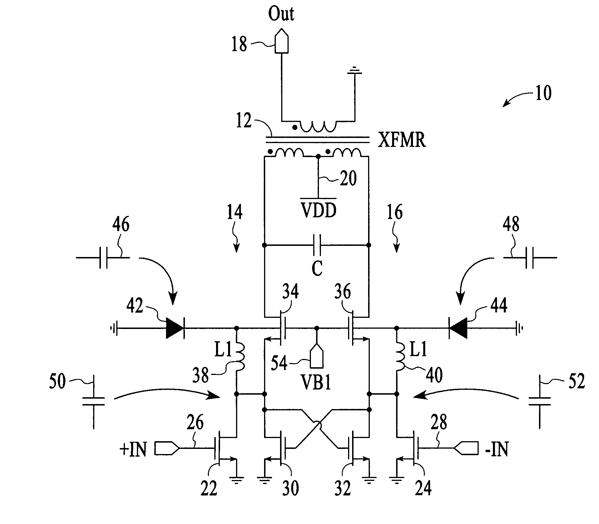
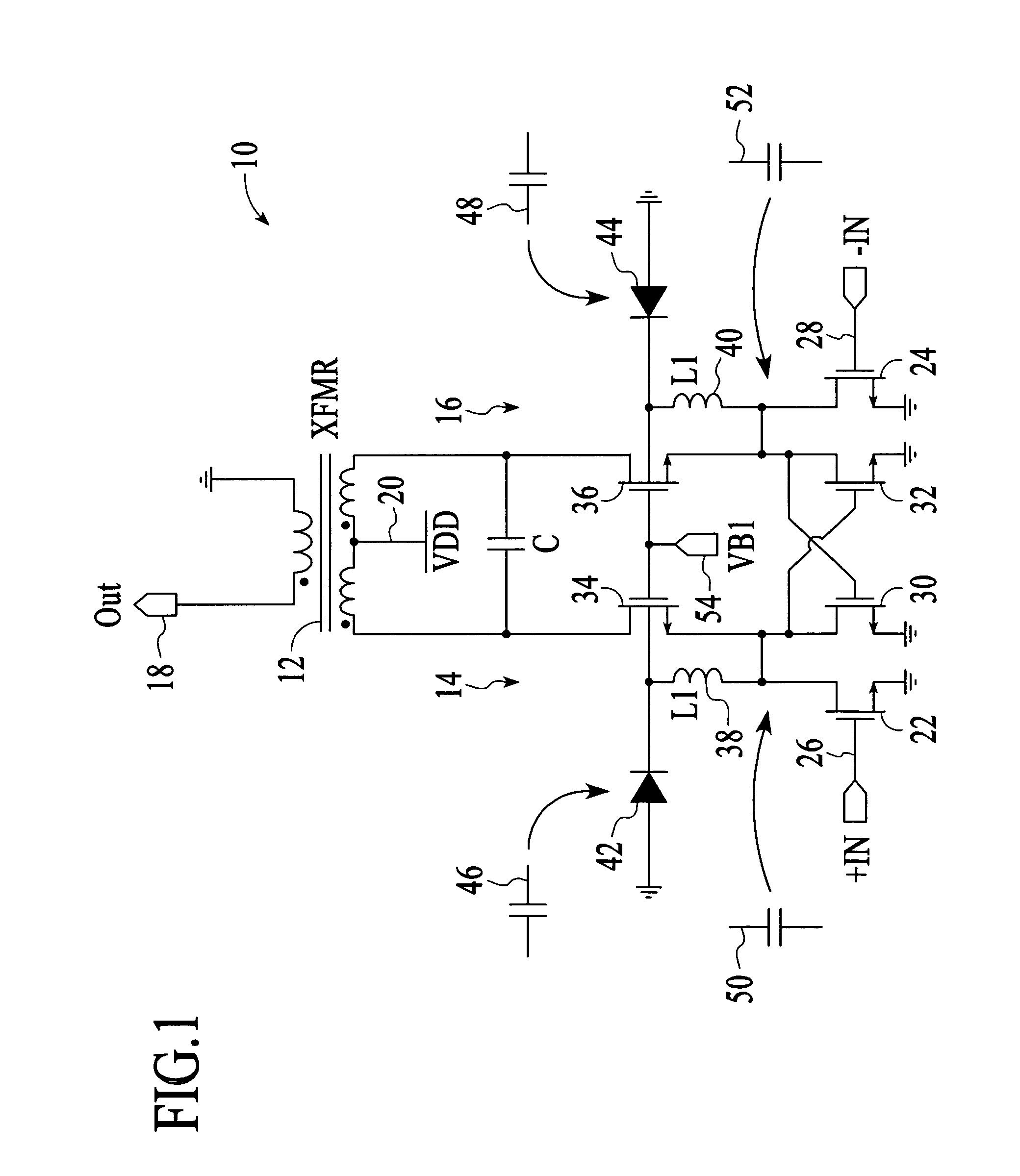
[0026]In the preferred embodiment of the invention, a cascode topology with deep-NWELL transistors is used to improve the breakdown voltage of a power amplifier 10. The approach allows for much higher signal swings at the power amplifier output, resulting in a higher transmitted power and an increased efficiency. As an additional feature, inductances may be added in order to resonate out excess capacitance at connections of transistors. While FIG. 1 shows one possible embodiment of the invention, modifications may be made without diverging from the invention. For example, the transformer 12 may be replaced with another type of impedance transforming network, such as a balun or a broadband transmission line transformer.

[0027]The embodiment of FIG. 1 employs a differential configuration in which a first amplifier stage 14 cooperates with a second amplifier stage 16 to define the RF amplifier output 18 at the secondary of the transformer 12. While not shown in FIG. 1, it is typical to ...


PUM


Abstract

A power amplifier utilizes cascode arrangements to achieve target performance levels for a power amplifier, such as the type used in wireless communication devices. A negative resistance circuit is provided for the cascode arrangement such that high gain, or oscillation, is promoted during operation of the power amplifier. In one embodiment, the negative resistance circuit includes cross-coupling transistors. Various features are provided in order to reduce the susceptibility of the power amplifier to voltage breakdown while maintaining good performance.

Description

TECHNICAL FIELD[0001]The invention relates generally to signal processing and more particularly to providing power amplification to input signals.BACKGROUND ART[0002]There are a number of concerns which must be addressed in the design and fabrication of circuitry for power amplification, such as the power amplifier of a wireless communication device. For such a device, the concerns include ensuring sufficient gain, providing efficiency with respect to converting direct current (DC) power to radio frequency (RF) output power, establishing breakdown voltage conditions that are sufficiently high to enable long term use of the device, and achieving reliable on-off performance of switching circuitry in switching-class power amplifiers. Currently, there is a desire to use low cost, standard digital complementary metal oxide semi-conductor (CMOS) circuitry for radio functions. This desire magnifies potential problems, because CMOS circuitry typically has very low breakdown voltages.[0003]T...

Claims


Application Information

Patent Timeline
Patent Type & Authority Patents(United States)
IPC IPC(8): H03F3/45
CPCH03F1/22H03F3/189H03F3/602H03F3/45188H03F2200/541H03F2200/198
Inventor BURNS, LAWRENCE M.WOO, CHONG L.SZETO, CLEMENT
Owner QORVO INT PTE LTD
Learn More