Semiconductor laser element

a laser element and semiconductor technology, applied in the field of semiconductor laser elements, can solve problems such as catastrophic optical damage (cod) and other problems, and achieve the effects of enhancing the output power of laser light from the front edge 210, and enhancing the light output power of semiconductor lasers

Active Publication Date: 2006-06-27
KK TOSHIBA
View PDF6 Cites 2 Cited by
  • Summary
  • Abstract
  • Description
  • Claims
  • Application Information

AI Technical Summary

Benefits of technology

[0009]The Inventor, however, had doubts in the conventional belief that lasers should be enhanced in property of light output power as their bandgaps of the window regions 212, 222 are widened from a result of simulation. Thus for the purpose of further enhancing light output power of semiconductor lasers, the Inventor repeated simulations and experiments under various conditions. As a result, it has been found that the bandgap of the front window region 212 had better be widened to the extent not adversely affecting the operation; however, by limiting the band gap of the rear window region 222 within a certain range, output power of laser light from the front edge 210 can be enhanced. Additionally, it has been confirmed that, within this range, unlikeness of occurrence of optical damage of the rear edge 220 is substantially equivalent to conventional lasers. That is, the Inventor has got the knowledge that, if the band gap of the rear window region 222 is narrowed toward the emission region 232 than the front window region 212, then the semiconductor laser can be enhanced in light output power than conventional lasers while ensuring reliability equivalent to conventional lasers.

Problems solved by technology

When such lasers are enhanced in output power, the issue of catastrophic optical damage (COD) arises.

Method used


Image

  • Semiconductor laser element
  • Semiconductor laser element
  • Semiconductor laser element

Examples


first embodiment

(First Embodiment)

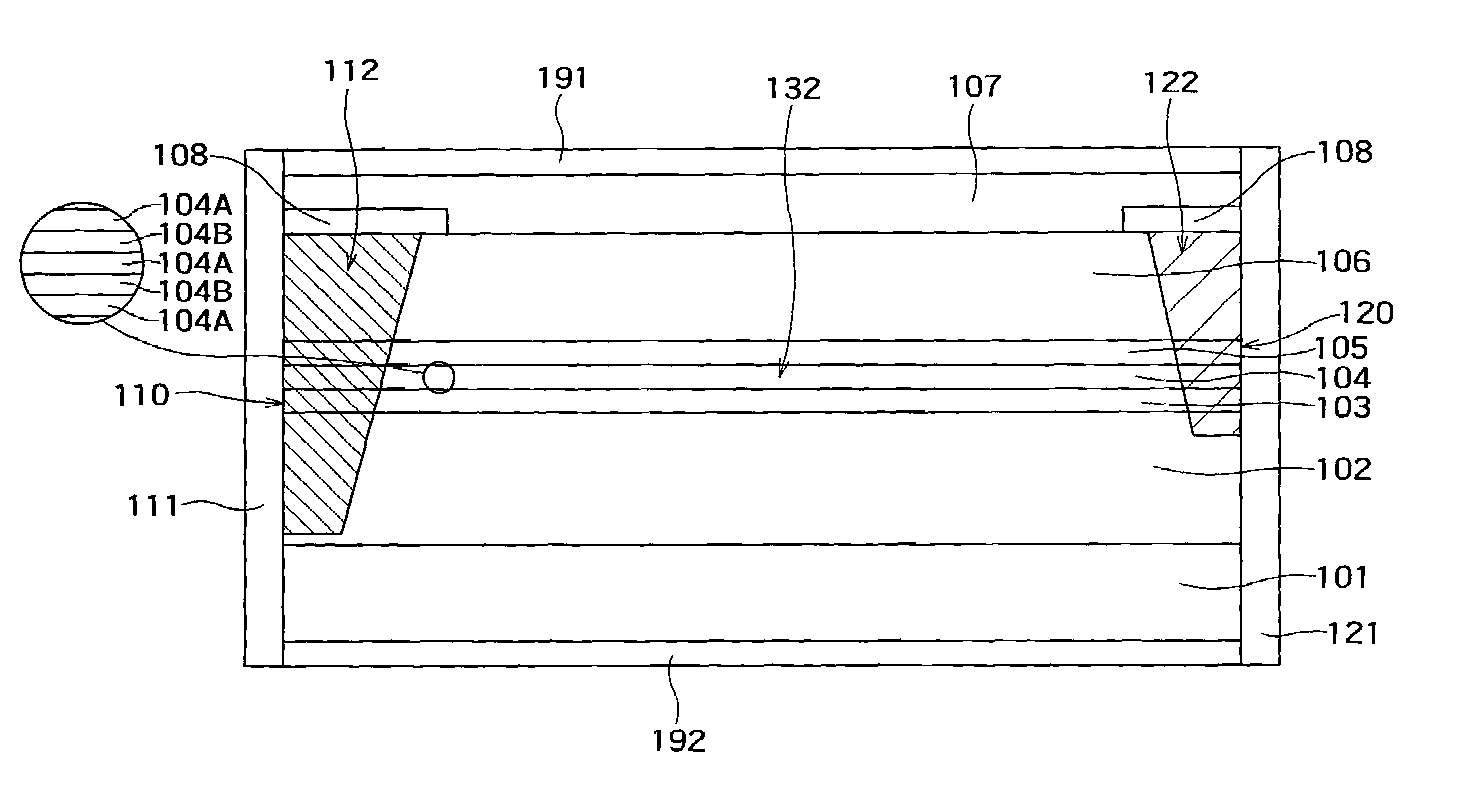
[0031]FIG. 1 is a cross-sectional view of a semiconductor laser element according to the first embodiment of the present invention. On an n-type GaAs substrate 101, there are sequentially formed an n-type clad layer 102 of In0.5(Ga0.3Al0.7)0.5P, guide layer 103 of In0.5(Ga0.4Al0.6)0.5P, active layer 104, guide layer 105 of In0.5(Ga0.4Al0.6)0.5P, p-type clad layer 106 of In0.5(Ga0.3Al0.7)0.5P, and p-type contact layer 107 of GaAs. The active layer 104 has a multiple well structure alternately stacking well layers 104A of In0.5Ga0.5P and barrier layers 104B of In0.5(Ga0.5Al0.5)0.5P. The active layer 104 is supplied with a current injected from a p-side electrode 191 shown as the top layer and an n-side electrode 192 shown as the bottom layer in the figure. With the injection of the current, the active layer emits light of a wavelength from 600 to 700 nm from its emission region 132 toward the front edge (first edge) 110 on the left and the rear edge (second edge) 120...

second embodiment

(Second Embodiment)

[0046]FIG. 4 is a cross-sectional view of a semiconductor laser element according to the second embodiment of the invention. The element of FIG. 4 has a structure similar to the element according to the first embodiment (FIG. 1), but made by first forming the layers up to the In0.5(Ga0.3Al0.7)0.5P p-type clad layer 106 by crystal growth, thereafter forming the window regions 112, 122, then forming a current blocking layer 108 of n-type GaAs to minimize the current flow into the window regions 112, 122, and thereafter forming the p-type contact layer 107 on the entire surface. In the other respects of the structure, the element shown here is substantially the same as the element according to the first embodiment (FIG. 1), and details thereof are not explained here.

[0047]In the structure of FIG. 4, the current blocking layer 108 contributes to more reliably reducing the current injection into the window regions 112, 122 and more reliably preventing the rise of tempe...


PUM

PropertyMeasurementUnit
reflectanceaaaaaaaaaa
lengthaaaaaaaaaa
lengthaaaaaaaaaa

Abstract

A semiconductor laser element, enhanced in light output power without decreasing the reliability, has a window structure including window regions wider in bandgap than the emission region of the laser, in which the bandgap of the rear window region is narrower than the bandgap of the front window region.

Description

CROSS-REFERENCE TO RELATED APPLICATIONS[0001]This application is based upon and claims the benefits of priority from the prior Japanese Patent Application No. 2002-247452, filed on Aug. 27, 2002, the entire contents of which are incorporated herein by reference.BACKGROUND OF THE INVENTION[0002]1. Field of the Invention[0003]The present invention relates to a semiconductor laser element, and more particularly, to a semiconductor laser element of a window structure for enhanced light output power.[0004]2. Related Background Art[0005]Recently, semiconductor laser elements using InGaAlP compound semiconductors for wavelengths from 600 nm to 700 nm have advanced to practical use in DVD (digital versatile disk), and have been enhanced in output power to be available for use as write lasers for recordable or rewritable DVD-RAM and others. When such lasers are enhanced in output power, the issue of catastrophic optical damage (COD) arises. Therefore, many lasers of this type have window reg...

Claims


Application Information

Patent Timeline
Patent Type & Authority Patents(United States)
IPC IPC(8): H01S5/00H01S5/16G11B7/125G11B7/127H01S5/028H01S5/343
CPCB82Y20/00G11B7/127H01S5/34326H01S5/162H01S5/028H01S5/3436H01S5/164H01S5/168
Inventor TANAKA, AKIRA
Owner KK TOSHIBA
Why Eureka
Try Eureka