Light emitting unit

a technology of light emitting unit and light source, which is applied in the direction of lighting and heating apparatus, semiconductor devices, light sources, etc., can solve the problems of limitation of the utilization of light emitted, and achieve the effect of improving the directional property of light emitted, increasing the light utilization of led, and improving the application field of light emitted

Active Publication Date: 2010-05-06
GIO OPTOELECTRONICS CORP
View PDF5 Cites 21 Cited by
  • Summary
  • Abstract
  • Description
  • Claims
  • Application Information

AI Technical Summary

Benefits of technology

[0013]As mentioned above, the light emitting unit of the present invention has the LED disposed between the substrate and a reflective element, and at least one part of the substrate is light permeable. Consequently, the reflective element with small diameter can reflect the light emitted from the surface of the LED, and the reflected light can pass through the substrate. The reflective element with small diameter can also concentrate the light passing through the substrate within a smaller diameter, which is advantageous for the following light reflecting or focusing design. The light emitted from the rear side of the LED may pass through the substrate and then be outputted to outside, so that the light utilization of the LED can be increased. Moreover, the lens element or another reflective element is disposed on the other side of the substrate for controlling the traveling direction of the light that passes through the substrate. This feature can improve the directional property of the light emitted from the light emitting unit. In addition, the configuration of the lens element or another reflective element, which is disposed on the other side of the substrate, can make the light emitting unit to be a transmissive type or a reflective type device, so that the application fields of the light emitting unit of the present invention can be broadened.
[0014]In addition, the light emitting unit of the present invention may have a plurality of reflective elements and LEDs that are disposed on different surfaces of a single substrate. This configuration allows the reflective elements and LEDs to be installed on, manufactured with, and / or inspected with the same substrate, so that the light emitting unit of the present invention can be easily manufactured in mass production.

Problems solved by technology

This also results in the limitation of the utilization of the light emitted from the LED 12.

Method used


Image

  • Light emitting unit
  • Light emitting unit
  • Light emitting unit

Examples


first embodiment

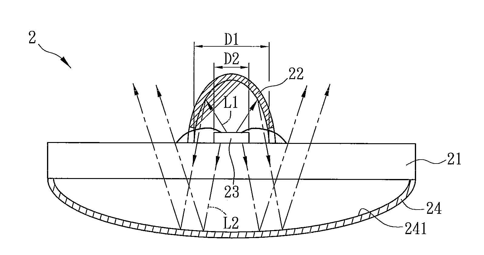
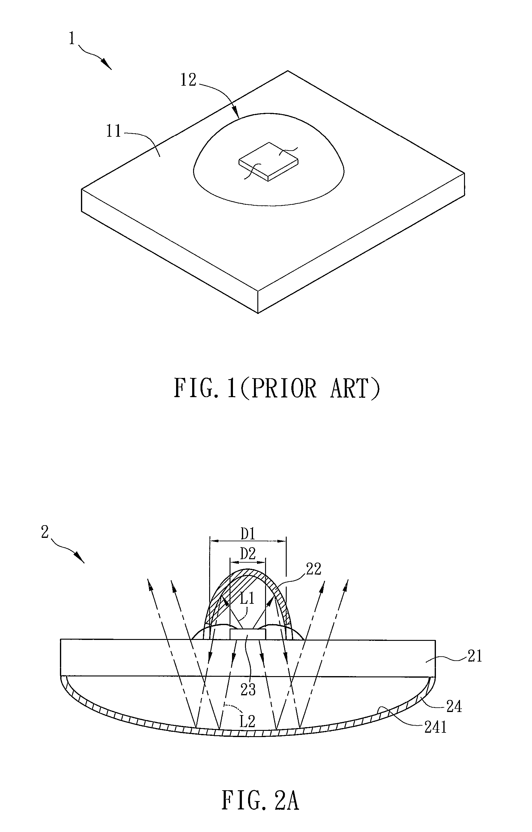
[0024]With reference to FIG. 2A, a light emitting unit 2 according to a first embodiment of the present invention includes a substrate 21, a first reflective element 22, a light-emitting diode (LED) 23, and a second reflective element 24.

[0025]At least one part of the substrate 21 is light permeable, and the material of the substrate 21 may include glass, sapphire, quartz, a polymer material, or a plastic material. In addition, the substrate 21 can be a circuit substrate (e.g. a glass circuit board).

[0026]The first reflective element 22 is, for example, a reflective plate or a reflective cup, and the material thereof can be metal, metal oxide, or white coating. If the first reflective element 22 is a reflective cap, the section thereof can be a planar surface or a curve surface. In this embodiment, the first reflective element 22 is a reflective cap with curved surface, and the curved surface may have one or more focuses. The maximum diameter D1 of the first reflective element 22 is...

second embodiment

[0041]FIG. 4 is a schematic diagram of a light emitting unit 3 according to a second embodiment of the present invention. With reference to FIG. 4, the light emitting unit 3 includes a substrate 31, a first reflective element 32, a LED 33, a second reflective element 34, and a molding body or an insulation layer 36. In this embodiment, the features and functions of the substrate 31, the LED 33 and the second reflective element 34 are the same as those of the substrate 21, the LED 23 and the second reflective element 24 of the first embodiment, so the detailed descriptions thereof will be omitted.

[0042]The molding body or insulation layer 36 at least partially covers the LED 33 and is at least partially disposed between the first reflective element 32 and the LED 33. In this embodiment, the first reflective element 32 is a reflective layer that is formed on the molding body or insulation layer 36.

[0043]If the first reflective element 32 is made of metal, it can be formed by evaporati...

third embodiment

[0049]FIG. 5 is a schematic diagram of a light emitting unit 4 according to a third embodiment of the present invention. With reference to FIG. 5, the light emitting unit 4 includes a substrate 41, a reflective element 42, a LED 43 and a lens element 44. In this embodiment, the features and functions of the substrate 41, the reflective element 42 and the LED 43 are the same as those of the substrate 21, the first reflective element 22 and the LED 23 of the first embodiment, so the detailed descriptions thereof will be omitted.

[0050]The lens element 44 is disposed opposite to the reflective element 42 and is located on a light outputting surface 411 of the substrate 41. In other words, the reflective element 42 and the lens element 44 are disposed on two opposite sides of the substrate 41, respectively. The lens element 44 may be a convex lens, microlens, or Fresnel lens, and the lens element 44 and the substrate 41 can be integrally formed. In this embodiment, the lens element 44 is...


PUM


Abstract

A light emitting unit includes a substrate, a first reflecting element, a light-emitting diode (LED), and a second reflecting element. At least one part of the substrate is light permeable. The LED is disposed between the substrate and the first reflecting element, and the first and second reflecting elements are disposed on two opposite sides of the substrate, respectively.

Description

CROSS REFERENCE TO RELATED APPLICATIONS[0001]This Non-provisional application claims priority under 35 U.S.C. §119(a) on Patent Application No(s). 097141837 filed in Taiwan, Republic of China on Oct. 30, 2008, the entire contents of which are hereby incorporated by reference.BACKGROUND OF THE INVENTION[0002]1. Field of Invention[0003]The present invention relates to a light emitting unit.[0004]2. Related Art[0005]Since the light-emitting diode (LED) has the advantages of good brightness and power consumption, the application fields of the LED have been broadened accompanying with the technology development of the LED. For example, the LED can be used in an illumination apparatus or the backlight of a liquid crystal display (LCD) device.[0006]As shown in FIG. 1, a conventional light emitting unit 1 includes a circuit substrate 11 and a LED 12, which is disposed on the circuit substrate 11. The LED12 is electrically connected with the circuit layer (not shown) on the circuit substrate...

Claims


Application Information

Patent Timeline
Patent Type & Authority Applications(United States)
IPC IPC(8): H01L33/00
CPCH01L33/507H01L33/60F21K9/68
Inventor CHEN, KUO-TSOCHEN, TONY K.T.
Owner GIO OPTOELECTRONICS CORP
Why Eureka
Try Eureka