

Structure and method for placement, sizing and shaping of dummy structures
a technology of dummy structures and structures, applied in the direction of cad circuit design, semiconductor/solid-state device testing/measurement, instruments, etc., can solve the problems of device degradation, reduce yield, and process non-uniformity, and achieve the effect of improving yield and reliability in the fabrication of chips
- Summary
- Abstract
- Description
- Claims
- Application Information
AI Technical Summary
Benefits of technology
Problems solved by technology
Method used
Image

Examples
Embodiment Construction
[0019]Other than the inventive concept, the apparatus and methods for fabricating chips are well-known and are not described further herein. Also, like numbers on different figures represent similar elements.
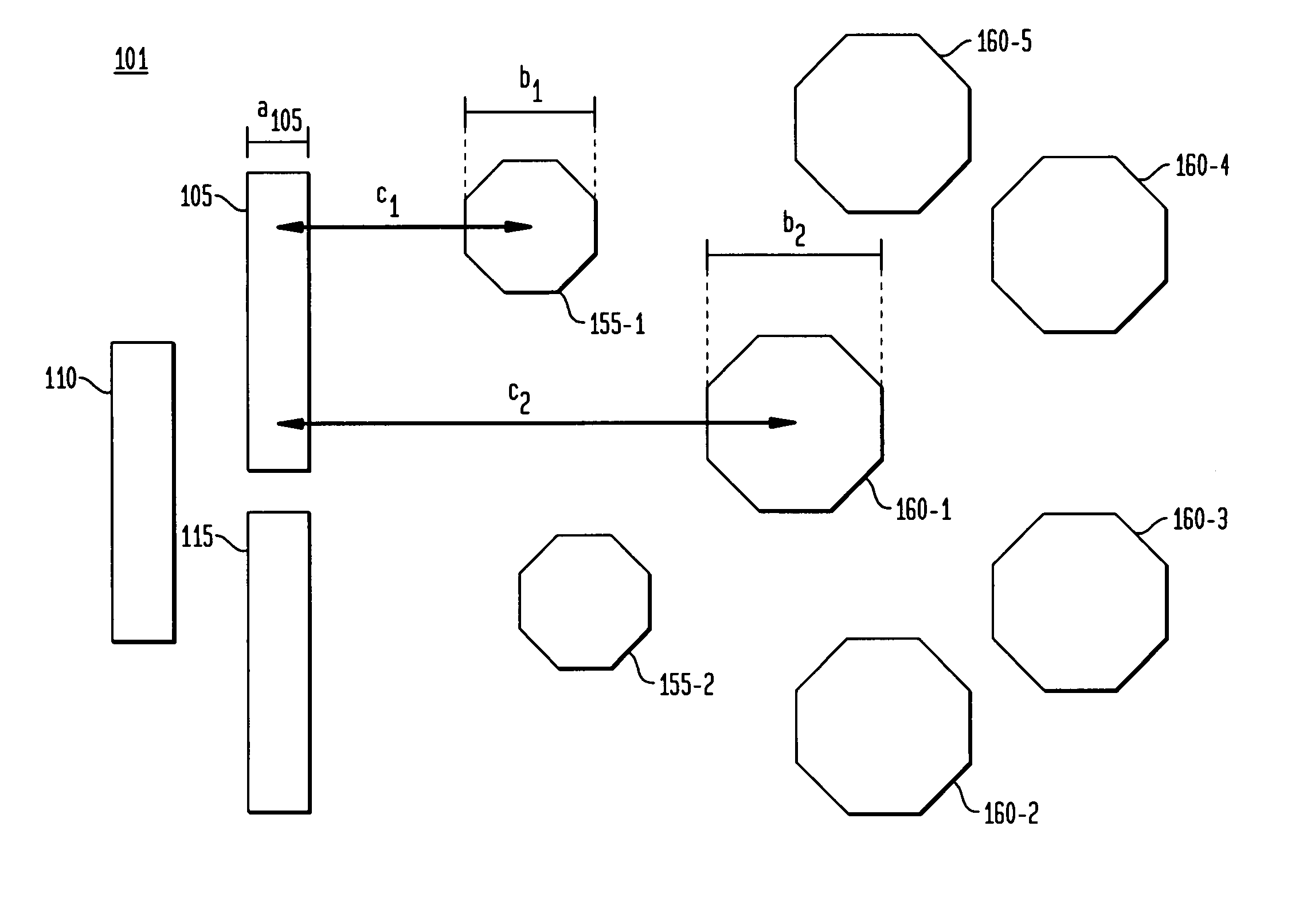
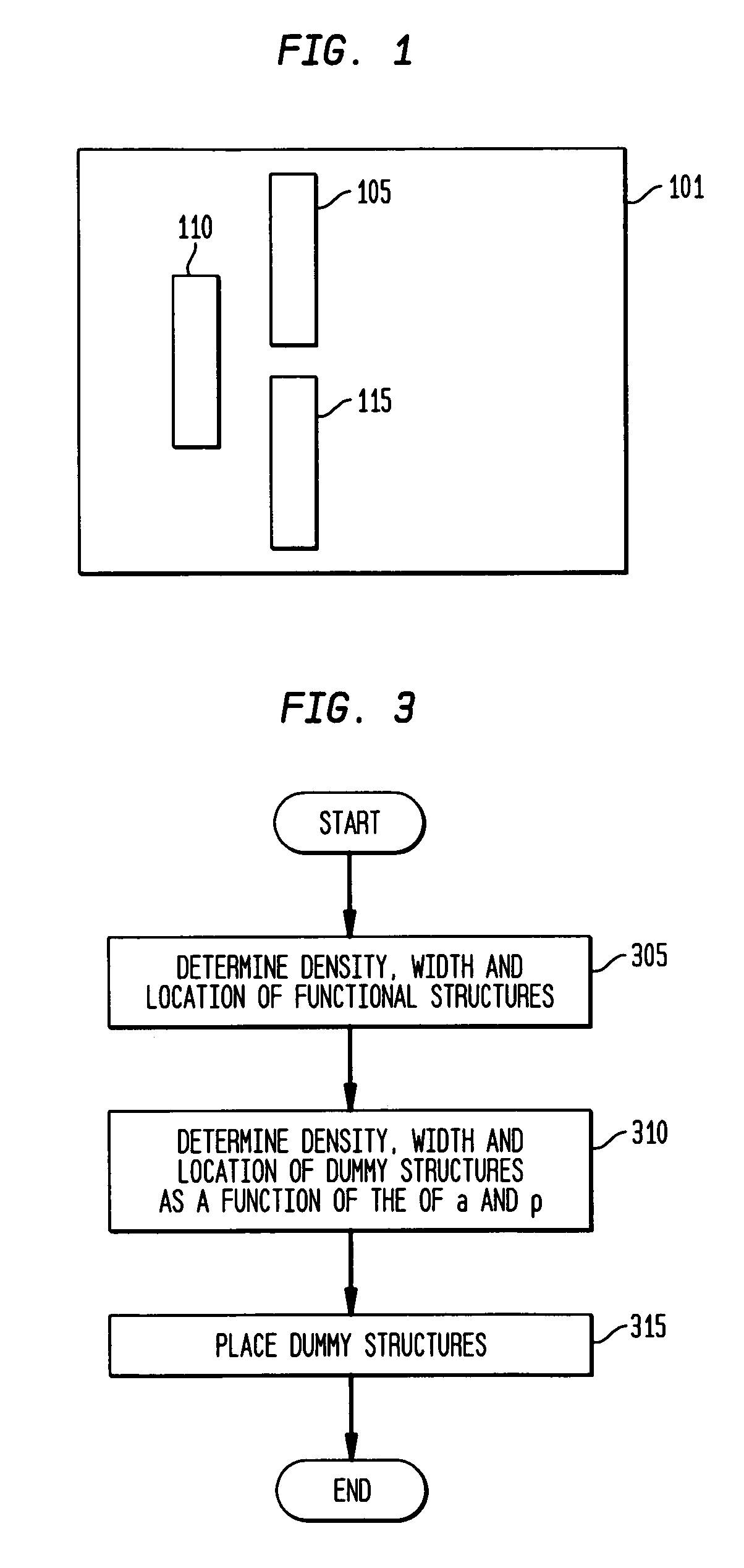
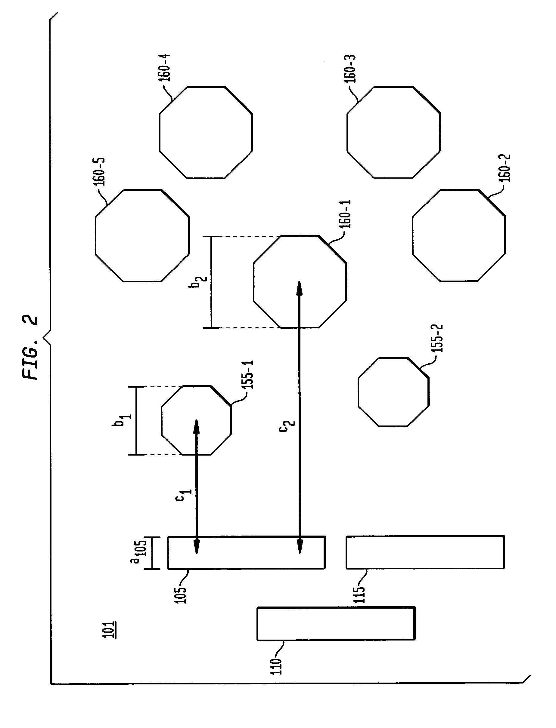
[0020]A top view of a representative layer 101 of an illustrative substrate 100 or formed on such substrate 100 is shown in FIG. 1. Illustratively, substrate 100 can be a semiconductor wafer, or can be any one of many different types of substrates on which processing is performed to pattern one or more layers thereof or formed thereon in the fabrication of microelectronic devices, MEMs and associated packaging. As defined herein, “layer” can be a layer formed on a substrate and can be portion or all of the substrate itself. Substrate 100 comprises three functional areas: 105, 110 and 115 arranged on layer 101. These functional areas represent raised areas of a layer 101 and may include, but are not limited to, one or more of the following: active elements, passive elements, and ...
PUM
 Abstract
Description
Claims
Application Information