Supply assembly for a led lighting module
- Summary
- Abstract
- Description
- Claims
- Application Information
AI Technical Summary
Benefits of technology
Problems solved by technology
Method used
Image
Examples
first embodiment
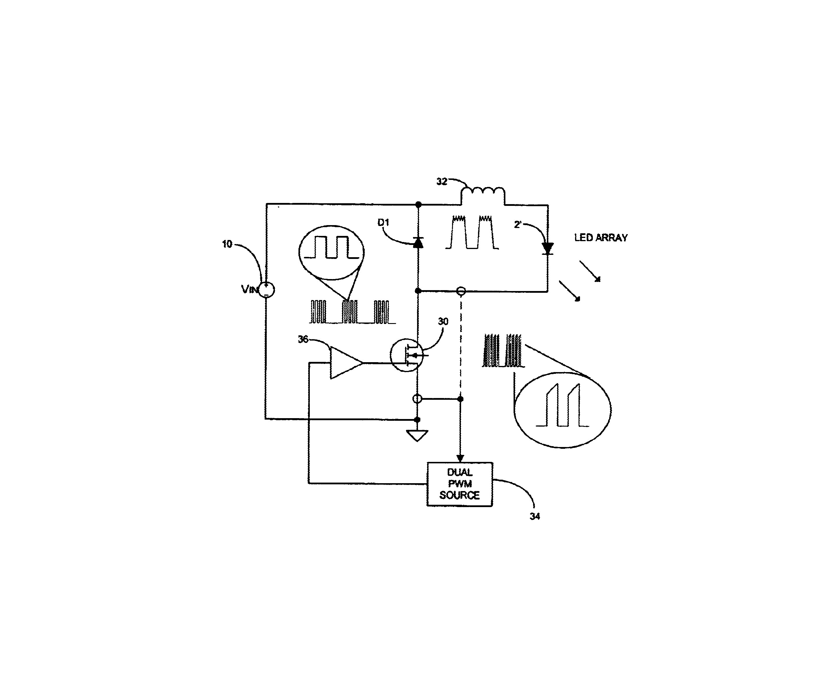
[0032]FIG. 9 shows the block circuit diagram of FIG. 7 with the controller 34. In particular, the controller 34 includes a current mode pulse width modulator 38 which receives an LED current reference signal from a current source 40, the sensed current, and a high frequency sawtooth signal. The current mode pulse width modulator 38 then supplies the high frequency pulse width modulated switching signal component which is applied to one input of an AND-gate 42, the other input of which receives the low frequency PWM switching signal component. The output from the AND-gate 42 is then applied through the amplifier 36 to the gate of the control switch 30.
second embodiment
[0033]FIG. 10 shows the block circuit diagram of FIG. 7, with the controller 34. In particular, the controller 34 includes an adder 44 having a positive input for receiving a reference voltage VREF and a negative input for receiving a high frequency ramp signal. An output from the adder 44 is applied to an inverting input of a comparator 46 which receives the sensed current at its non-inverting input. An output of the comparator 46 is applied to the reset input of an RS flip-flop 48 which receives a high frequency clock signal at its set input. The Q output from the RS flip-flop 48 is applied to one input of an AND-gate 50 which receives the low frequency PWM switching signal component at its other input. The output from the AND-gate 50 is then applied through the amplifier 36 to the gate of the control switch 30.
[0034]In the embodiment of FIG. 9, either peak or average current detection may be used, while in the embodiment of FIG. 10, peak current detection is used.
third embodiment
[0035]FIG. 11 shows the block circuit diagram of FIG. 7, showing the controller 34 in which both peak current detection and average current detection are used. In particular, the sensed current is applied to an integrator 52 which forms an average of the sensed current. An output of the integrator 52 is applied to a low frequency pulse width modulator 54 which receives a reference current from current source 56 and a low frequency sawtooth signal from low frequency sawtooth generator 58 which has a user control 60 coupled thereto. An output from the low frequency pulse width modulator 54 is applied to a first input of an AND-gate 62. The sensed current is also applied to a sample-and-hold circuit 64. An output from the sample-and-hold circuit 64, which represents the peak sensed current, is applied to a high frequency pulse width modulator 66 which also receives a reference current from current source 68 and a high frequency sawtooth signal from high frequency sawtooth generator 70....
PUM
 Abstract
Description
Claims
Application Information


