Optical switch

a technology of optical switch and waveguide, which is applied in the field of optical switch, can solve the problems of increasing the loss of light which is guided to the desired output channel waveguide, and achieve the effects of low loss, large deflection angle and low loss

Active Publication Date: 2006-07-04
FUJITSU LTD
View PDF9 Cites 3 Cited by
  • Summary
  • Abstract
  • Description
  • Claims
  • Application Information

AI Technical Summary

Benefits of technology

[0017]In the optical switch of the configuration as described above, the light input to the input channel waveguide is given to the first optical deflecting unit to be propagated within the slab type optical waveguide. To this slab type optical waveguide, the input side upper electrode portions and the output side upper electrode portions are disposed on the top surface thereof, and the lower electrode is disposed on the bottom surface thereof. When the light passes below the input side upper electrode portion, the respective lights of TE/TM modes are deflected at different angles due to the electro-optic effect based on the electric field generated between the input side upper electrode portion and the lower electrode by the application of voltage from the drive circuit. Then, the deflected lights pass through the mode conversion element to be subjected to the TE/TM mode conversion, and further, the inter-converted lights of TE/TM modes are deflected at different angles, in the same manner as that in the input side, when passing through the underside of the output side upper electrode portion. Thus, traveling directions of the respective lights of TE/TM modes output from the first optical deflecting unit to the slab type optical waveguide unit are made parallel to each other. The respective lights of TE/TM modes which have traveled straight in the slab type optical waveguide unit while maintaining the parallel state thereof, are given to the second optical deflecting unit...

Problems solved by technology

However, in the case where the material having the high electro-optic effect is used, since the polarization dependence of the deflectio...

Method used


Image

  • Optical switch
  • Optical switch
  • Optical switch

Examples


Embodiment Construction

[0029]Hereinafter, embodiments of the present invention will be described with reference to drawings. The same reference numerals denote the same or equivalent parts in all drawings.

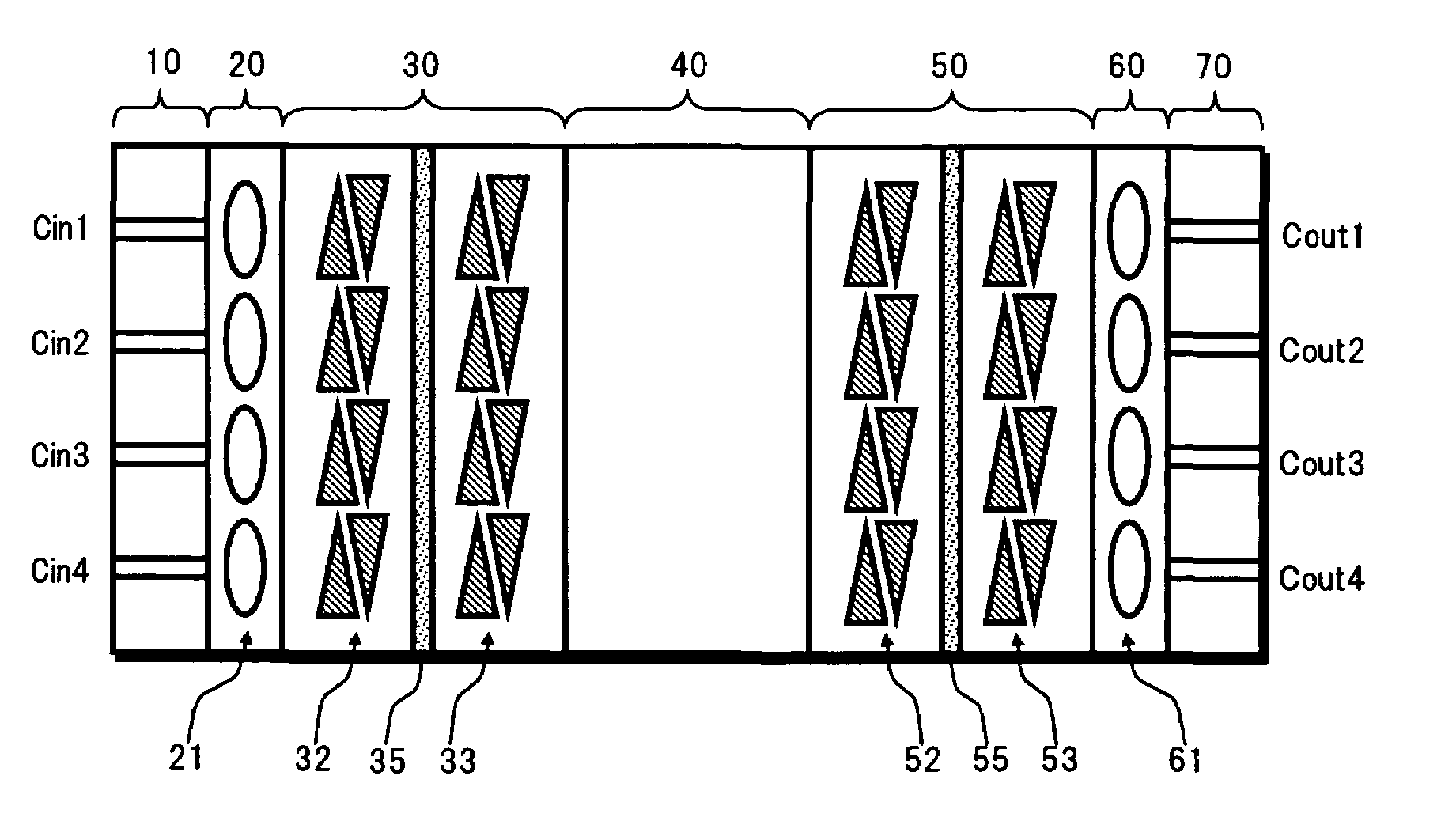
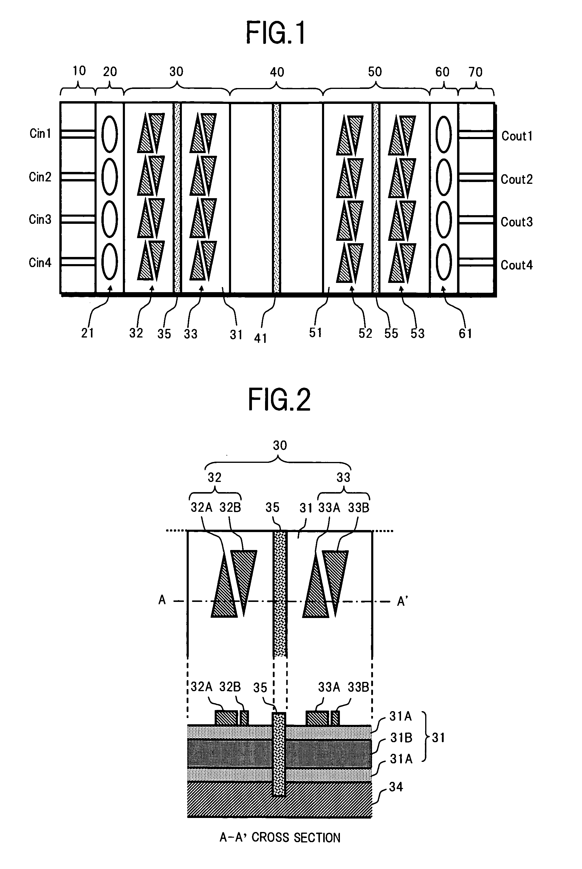
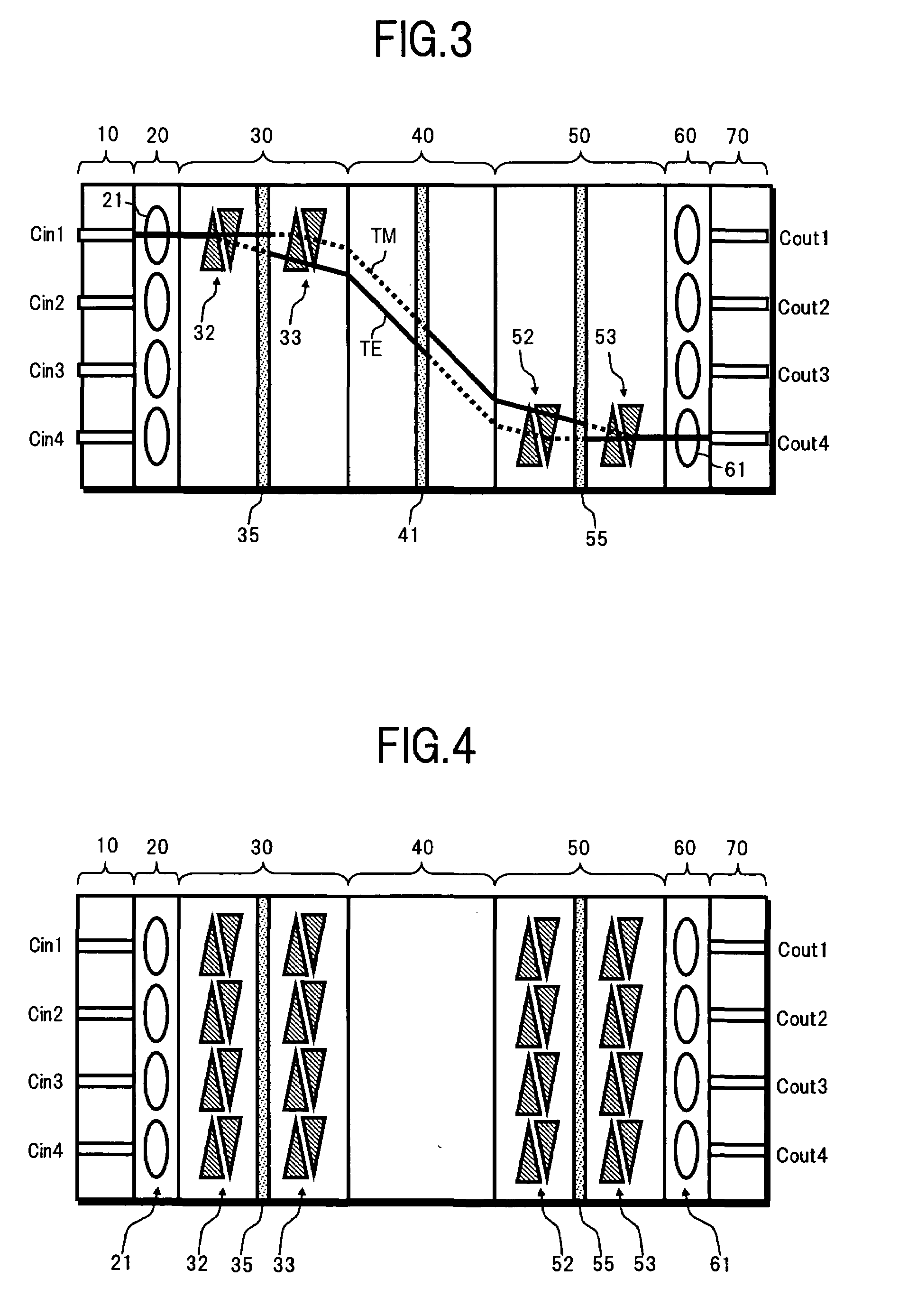
[0030]FIG. 1 is a top view showing a configuration of an optical switch according to the present invention.

[0031]In FIG. 1, the present optical switch comprises, for example: an optical input section 10; a collimate section 20; a first optical deflecting section 30 as first optical deflecting unit; a slab type optical waveguide section 40 as slab type optical waveguide unit; a second optical deflecting section 50 as second optical deflecting unit; an optical condensing section 60; and an optical output section 70.

[0032]The optical input section 10 is made up by forming a plurality (here, four, for example) of input channel waveguides Cin1 to Cin4 on a typical optical substrate. A light whose determination is switched by the present optical switch is incident on one end of each of the input channel wavegu...


PUM


Abstract

An optical switch of the present invention is for deflecting a light given to an input channel waveguide by first and second optical deflecting sections arranged respectively on the former and latter stages of a slab type optical waveguide section, so that a deflection angle by the first optical deflecting section is symmetrical to that by the second optical deflecting section, to guide the light to a desired output channel waveguide. The first and second optical deflecting sections each includes a half-wave plate between input side upper electrode portions and output side upper electrode portions each of which is formed with prism type electrodes, and the slab type optical waveguide also includes a half-wave plate on the center thereof. As a result, by forming an optical deflection element using a material having the polarization dependence and a high electro-optic effect, it becomes possible to achieve the reduction of drive voltage and an increase of deflection angle, and also, to reduce a loss occurred due to the polarization dependence of the deflection angle.

Description

BACKGROUND OF THE INVENTION[0001]1. Field of the Invention[0002]The present invention relates to an optical switch for switching paths between input channel waveguides and output channel waveguides, utilizing the deflection of optical beams.[0003]2. Description of the Related Art[0004]In recent years, the transmission band of optical communication has been enlarged, and the speeding up and large capacity thereof has been developed combined with the wavelength division multiplexing (WDM) technology. In order to construct hardware infrastructures of optical fiber network in a backbone communication network, an optical switch for switching transmission determinations of optical signals is required.[0005]As a conventional optical switch, there has been known an optical switch utilizing a movable micro-mirror. Further, in order to further develop the high integration and high-speed of the optical switch, the development of optical switches utilizing a change in the refractive index due t...

Claims


Application Information

Patent Timeline
IPC IPC(8): G02B6/26G02B6/42
CPCG02F1/313
Inventor SHIRAISHI, TAKASHI
Owner FUJITSU LTD
Why Eureka
Try Eureka