
Optical module and manufacturing method therefor

a technology of optical modules and manufacturing methods, applied in the field of optical modules, can solve the problems of increasing propagation loss, difficult to efficiently make direct connection between optical waveguides and general optical fibers, and affecting the efficiency of optical waveguides, and achieve the effect of high efficiency

Active Publication Date: 2006-07-11
NIPPON TELEGRAPH & TELEPHONE CORP
View PDF24 Cites 23 Cited by
  • Summary
  • Abstract
  • Description
  • Claims
  • Application Information

AI Technical Summary

Benefits of technology

[0010]It is, therefore, a principal object of the present invention to provide an optical module which can realize light propagation between optical waveguides having different mode field sizes with high efficiency, and a manufacturing method for the optical module.
[0011]It is another object of the present invention, in addition to the principal object, to provide an optical module which can reduce a connection loss more than the prior art, and a manufacturing method for the optical module.
[0012]It is still another object of the present invention to provide a manufacturing method for an optical module, which can manufacture an optical module with higher precision and a smaller number of steps than in the prior art.
[0013]It is still another object of the present invention to provide a manufacturing method for an optical module with a high degree of margin for processing.
[0014]It is still another object of the present invention to provide a manufacturing method for an optical module, which can manufacture an optical module without damaging a previously formed portion.

Problems solved by technology

Problems are posed in connection between these optical waveguides and optical fibers, light-emitting devices, light-receiving devices, and the like in terms of the respective mode field sizes (diameters).
It is therefore difficult to efficiently make direct connection between an optical waveguide and a general optical fiber or the like having a large mode field size.
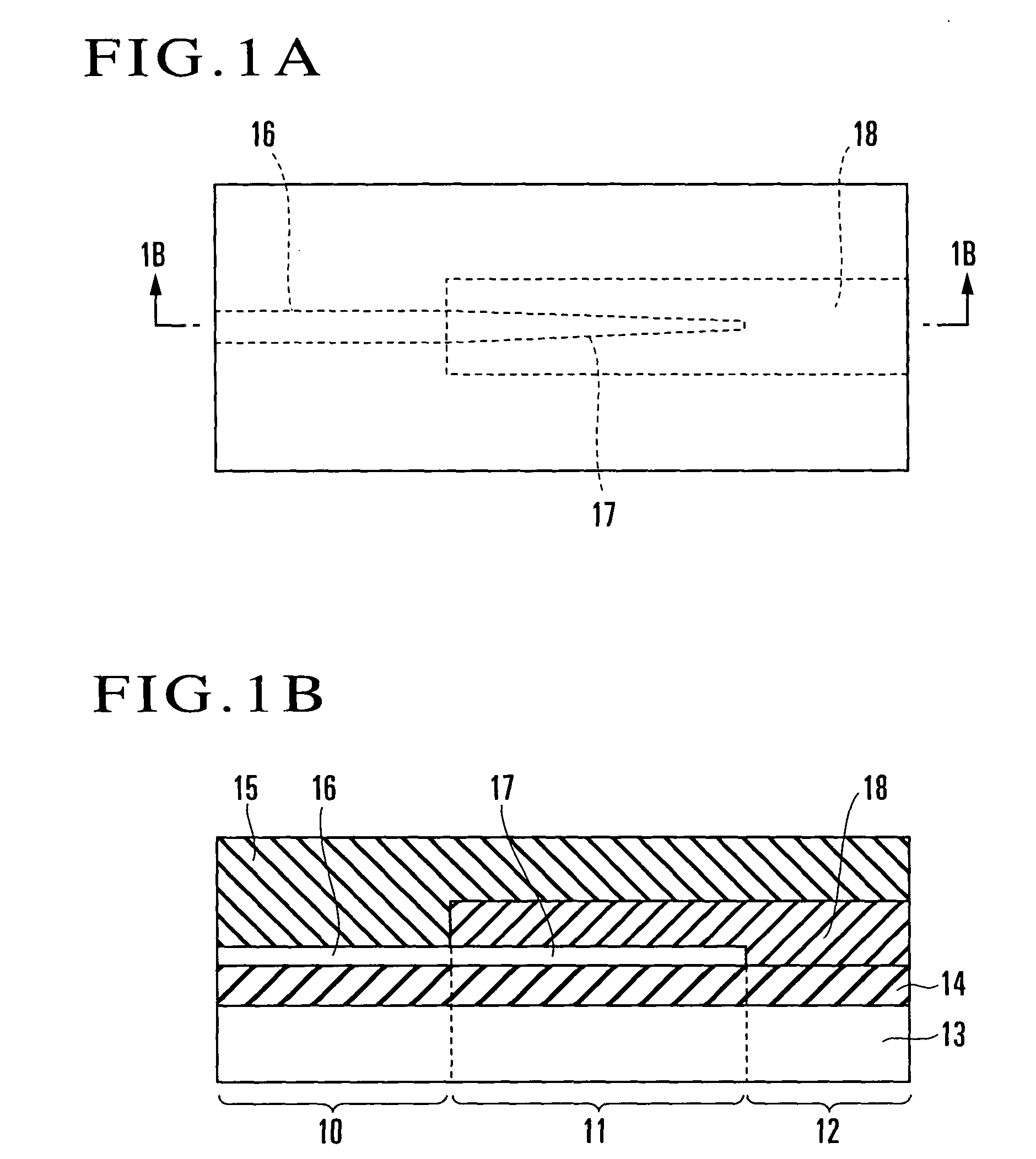
In addition, since there is no over cladding layer around the core 16 of the first optical waveguide 10 made of a silicon wire, the core 16 of the optical waveguide 10 tends to be damaged, resulting in an increase in propagation loss.
It is therefore difficult to economically process tapered portions.

Method used


Image

  • Optical module and manufacturing method therefor
  • Optical module and manufacturing method therefor
  • Optical module and manufacturing method therefor

Examples


first embodiment

(First Embodiment)

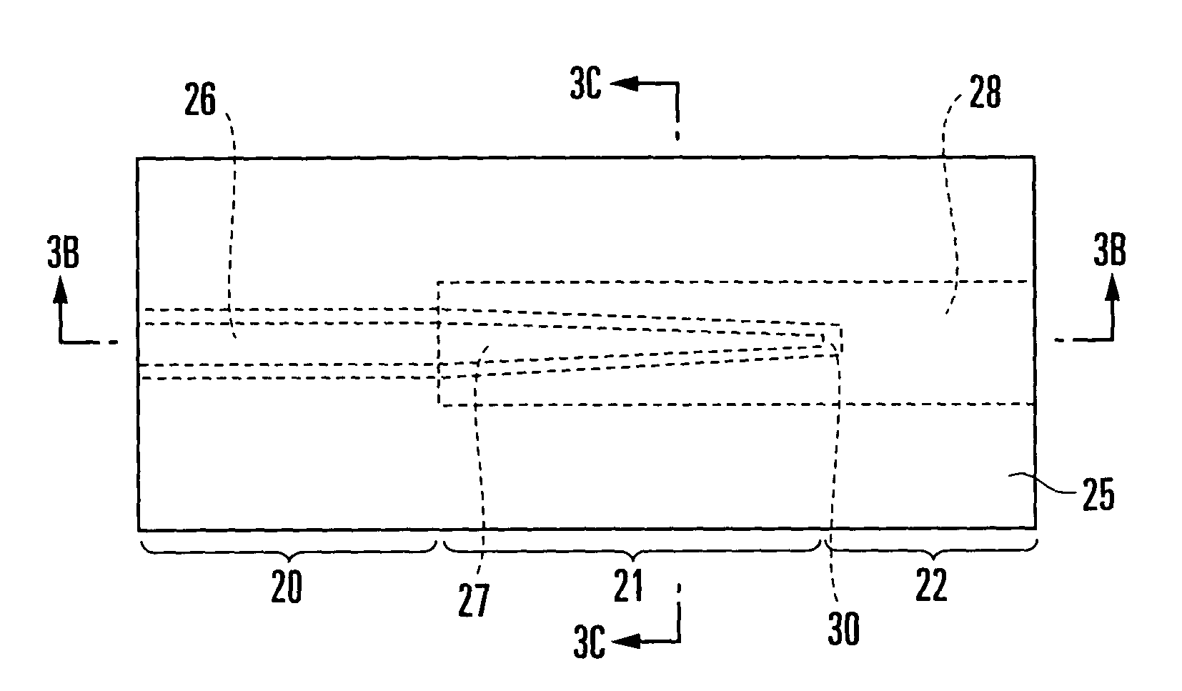
[0054]FIGS. 3A to 3C show an optical module according to the first embodiment of the present invention. Referring to FIGS. 3A to 3C, reference numeral 20 denotes a wire-like first optical waveguide made of silicon; 21, a mode field size conversion portion; 22, a second optical waveguide connected to the first optical waveguide 20; 23, a silicon substrate; 24, an under cladding formed from a silicon oxide film and placed on the silicon substrate 23; 25, an over cladding made of a polymer; 26, a first core which is made of silicon and forms the first optical waveguide 20; 27, a tapered portion which is made of silicon like the first core 26 and formed such that the width dimension decreases toward its distal end while the height of a cross section (thickness) of the core 26 is kept unchanged; 28, a second core which is made of a polymer and formed as the core of the mode field size conversion portion 21 and second optical waveguide 22; and 30, a silicon oxide film.

[0...

second embodiment

(Second Embodiment)

[0073]FIGS. 7A to 7C show an optical module according to the second embodiment of the present invention. The same reference numerals as in FIGS. 3A to 3C denote the same part in FIGS. 7A to 7C. A characteristic feature of this embodiment is that a silicon oxide film 30 is formed to be adjacent to only the side surfaces of a tapered portion 27. This allows the tapered portion 27 to be shaped with high precision.

[0074]A manufacturing method for the optical module shown in FIGS. 7A to 7C will be described below with reference to FIGS. 8A to 8G.

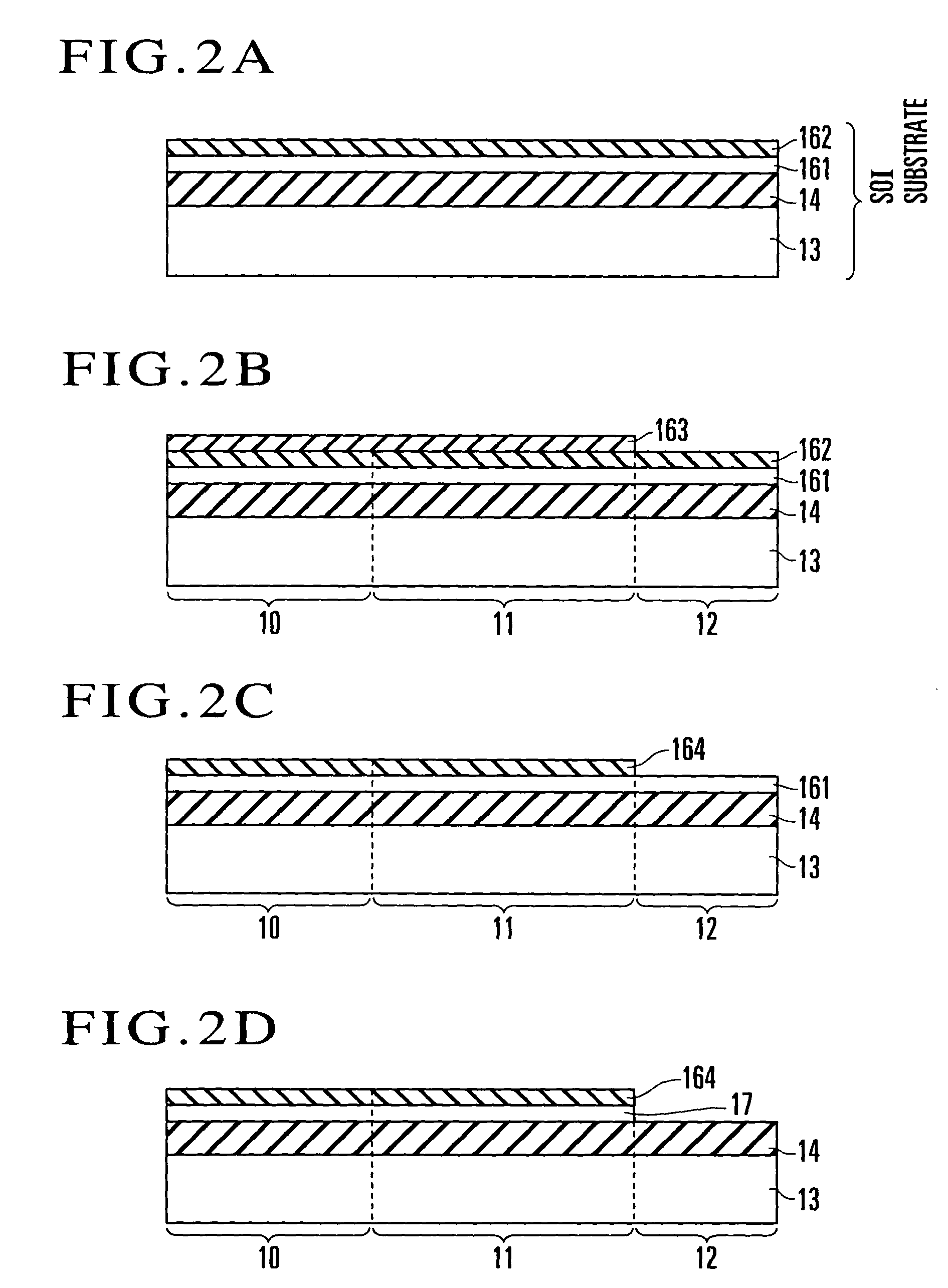
[0075]The steps in FIGS. 8A to 8D are the same as those in FIGS. 4A to 4D in the first embodiment. In the first embodiment, the first core 26 of the first optical waveguide 20 and the tapered portion 27 continuous with the core 26 are formed by etching the silicon layer 31 by using the mask 29, and an oxidation process is performed after the mask 29 is removed. In this embodiment, an oxidation process similar to that in the fir...

third embodiment

(Third Embodiment)

[0083]This embodiment is a modification of the manufacturing method for the optical module shown in FIGS. 4A to 4H, and exemplifies only the part of the method, in particular, in which after a silicon layer serving as the first core is formed on an under cladding, a silicon oxide film is formed to cover the first core. The use of this embodiment makes it possible to manufacture an optical module in a shorter period of manufacturing time than the conventional method.

[0084]Referring to FIGS. 9A to 9C, reference numeral 111 denotes a silicon substrate; 112, an under cladding layer formed from a silicon oxide film (SiO2); and 113, a core serving both as the first core of the first optical waveguide and the tapered portion in the first embodiment described above. The core 113 is made of silicon and patterned into a thin wire. Reference numeral 114 denotes a silicon oxide film placed to cover the core 113. In this case, the width and thickness of the core 113 are differe...


PUM


Abstract

An optical module includes an under cladding, a first core, a second core, and an over cladding. The under cladding has a flat shape as a whole. The first core has a quadrangular cross section and is placed on the under cladding. The second core is placed on a terminal end portion of the first core. The over cladding is placed in a region including the terminal end portion of the first core and the second core placed on the terminal end portion of the first core. The under cladding and the first core placed thereon constitute a first optical waveguide. The under cladding, the terminal end portion of the first core placed on the under cladding, the second core placed thereon, and the over cladding placed on and around the second core constitute a mode field size conversion portion. The under cladding, the second core placed on the under cladding, and the over cladding placed on and around the second core constitute a second optical waveguide. The first core is made of silicon. The first and second cores differ in cross-sectional shape. A manufacturing method for the optical module is also disclosed.

Description

BACKGROUND OF THE INVENTION[0001]The present invention relates to an optical module used in the optoelectronic field and optical communication field, and a manufacturing method for the optical module.[0002]Recently, for miniaturizing optical circuits, various researches and developments have been conducted on silicon wire optical waveguides using SOI (Silicon On Insulator) substrates and photonic crystal waveguides. Problems are posed in connection between these optical waveguides and optical fibers, light-emitting devices, light-receiving devices, and the like in terms of the respective mode field sizes (diameters). These optical waveguides have mode field sizes on the submicron order, whereas optical fibers and the like have mode field sizes on the order of several microns. It is therefore difficult to efficiently make direct connection between an optical waveguide and a general optical fiber or the like having a large mode field size. In order to connect them with a low loss, a m...

Claims


Application Information

Patent Timeline
Patent Type & Authority Patents(United States)
IPC IPC(8): G02B6/26G02B6/10G02B6/42G02B6/12G02B6/122G02B6/30
CPCG02B6/1228G02B6/305G02B2006/12176
Inventor YAMADA, KOJITSUCHIZAWA, TAIUCHIYAMA, SHINGOSHOJI, TETSUFUMITAKAHASHI, JYUN-ICHIWATANABE, TOSHIFUMITAMECHIKA, EMIMORITA, HIROFUMI
Owner NIPPON TELEGRAPH & TELEPHONE CORP
Learn More