High-frequency device, high-frequency module and communications device comprising them

a high-frequency module and communication device technology, applied in the field of wireless communication system, can solve the problems of not teaching any specific means for solving deterioration, circuit parts containing high-power amplifiers have not been formed into a single laminate module, and mobile phones are sometimes disconnected, so as to maximize harmonic attenuation and minimize insertion loss

Active Publication Date: 2006-07-11
MURATA MFG CO LTD
View PDF13 Cites 35 Cited by
  • Summary
  • Abstract
  • Description
  • Claims
  • Application Information

AI Technical Summary

Benefits of technology

[0013]Accordingly, an object of the present invention is to provide a high-frequency device comprising a phase-adjusting circuit between a switch circuit a...

Problems solved by technology

According to recent rapid expansion of mobile phones, however, a frequency band allocated to each system cannot allow all users to use their mobile phones in major cities in advanced countries, resulting in difficulty in connection and thus causing such a problem that mobile phones are sometimes disconnected during communication.
However, circuit parts containing high-power amplifiers have not been formed into a single laminate module.
However, this reference teaches nothing about problems arising when the high-frequency switches and the amplifiers are integrated, and their solution means.
However, this reference does not teach any specific means for solving the deterioration of the characteristics of reducing insertion loss between the high-frequency parts and harmonic attenuation characteristics.
When the high-fre...

Method used


Image

  • High-frequency device, high-frequency module and communications device comprising them
  • High-frequency device, high-frequency module and communications device comprising them
  • High-frequency device, high-frequency module and communications device comprising them

Examples


first embodiment

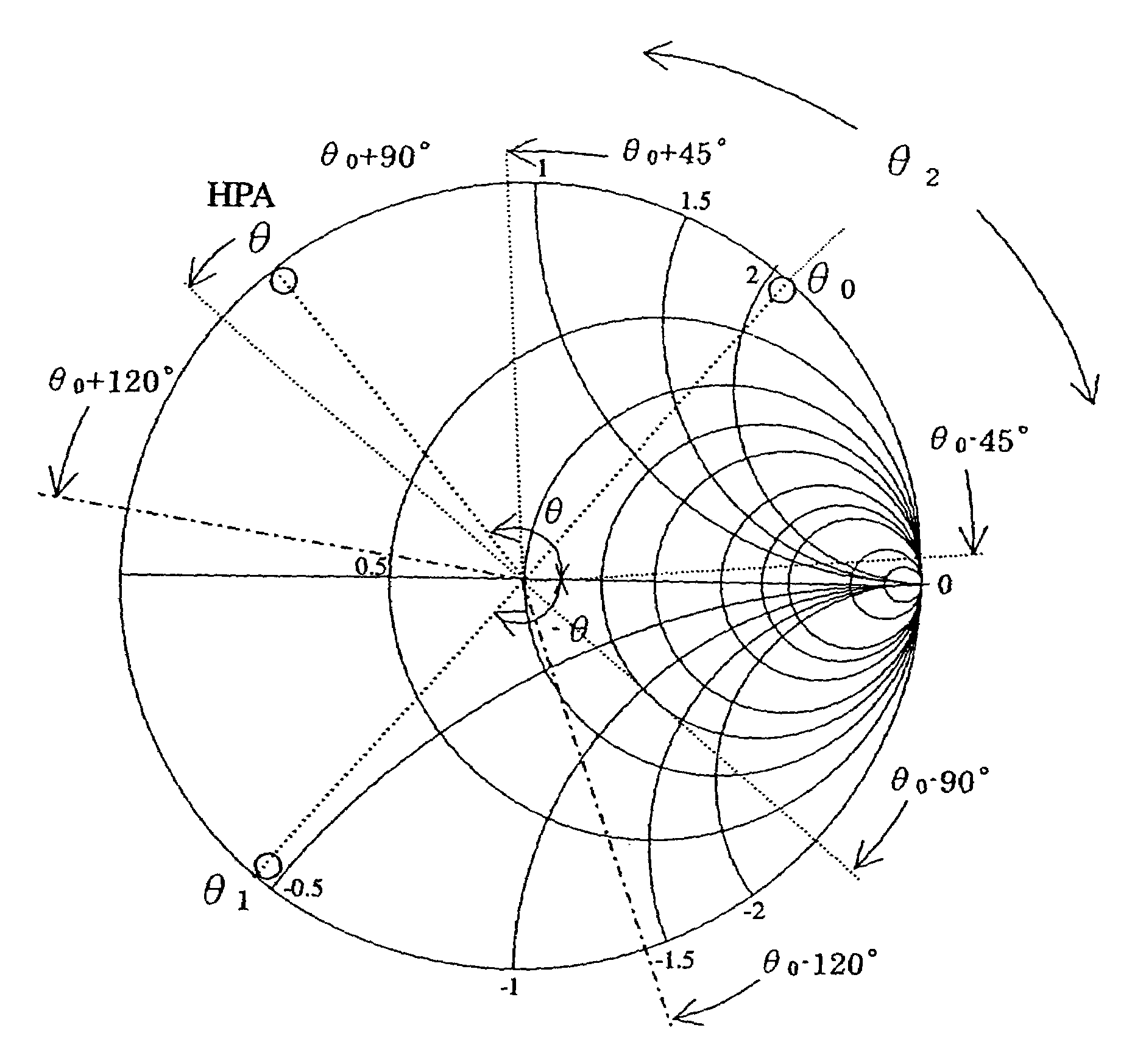
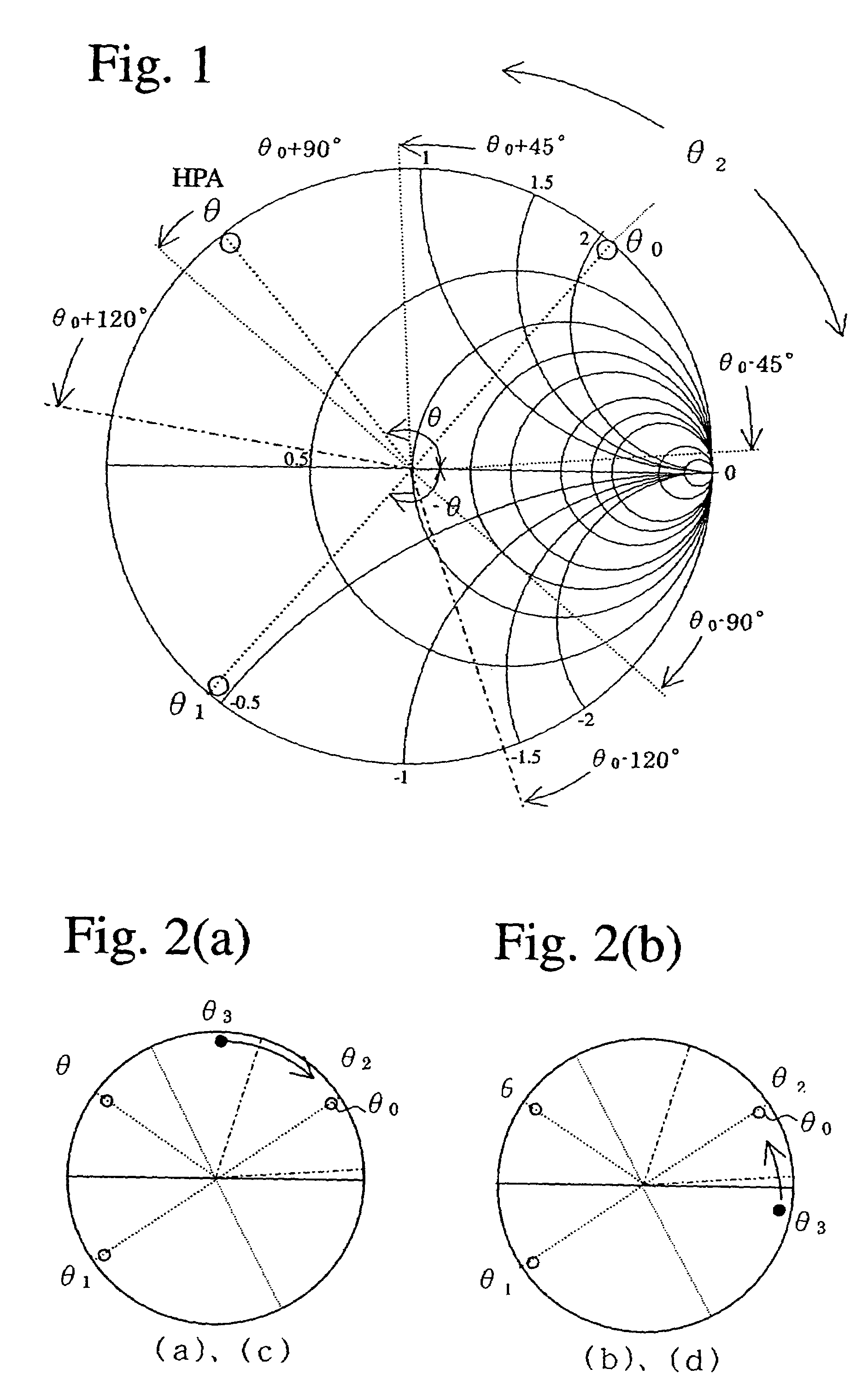
[0120]This embodiment uses a semiconductor chip having a function of monitoring an output power. FIG. 11 shows the equivalent circuit of a triple-band antenna switch module part for EGSM, DCS and PCS. FIG. 12 shows the equivalent circuit of a high-frequency amplifier, and FIGS. 13(a) and (b) show their circuit portions near the connection points. The high-frequency module of this embodiment is constituted by apparatuses (ASM +HPA) in a range shown by the solid line in FIG. 23, which are combined in one laminate, and FIG. 17 is a partial development view showing the laminate.

(A) Diplexer (Branching Circuit)

[0121]Referring to FIG. 11, the diplexer Dip is constituted by transmission lines L1–L4 and capacitors C1–C4. The transmission line L2 and the capacitor C1 constitute a series resonance circuit designed to have a resonance frequency in a DCS band (transmission frequency: 1710–1785 MHz, receiving frequency: 1805–1880 MHz) and a PCS band (transmission frequency: 1850–1910 MHz, receiv...

second embodiment

[0133]The EGSM system may be divided to GSM850 (transmission frequency: 824–849 MHz, receiving frequency: 869–894 MHz) and EGSM, to provide a quadruple-band, high-frequency device. In this case, the transmitting system comprises a common terminal, and the receiving system comprising a triple-band antenna switch, whose EGSM-receiving terminal is connected to a switch for switching GSM850 and EGSM. A frequency between them can be divided by a transmission line, a λ / 4 resonator of a GSM850 band and an EGSM band, in place of this switch.

(A) High-frequency Amplifier

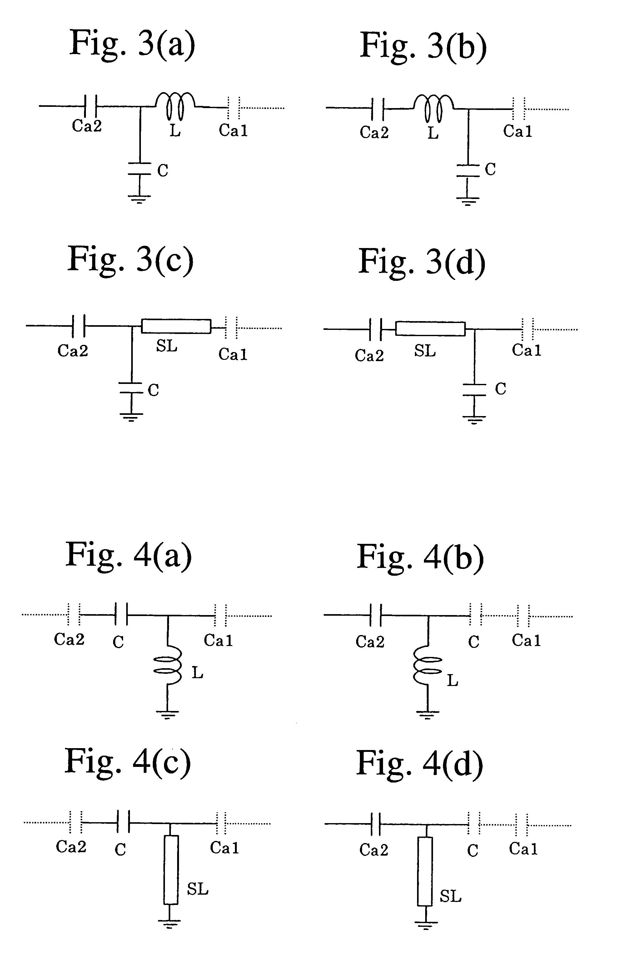
[0134]FIG. 12 shows one example of a matching circuit in the high-frequency amplifier constituting the high-frequency device. An output terminal P0 of this matching circuit is connected, for instance, to a transmission terminal P1 of EGSM Tx in the antenna switch module of FIG. 6, to send the amplified transmission signal to the antenna switch. The output terminal P0 is connected to one end of the transmission line ASL1 via th...

third embodiment

(High-frequency Module)

[0145]FIG. 17 is a development view showing green sheets in upper first to third layers, intermediate seventh to eighth layers and lower thirteenth to fifteenth layers, in a high-frequency module containing the antenna switch module part having the equivalent circuit of FIG. 11 and the high-frequency amplifier part having the equivalent circuit of FIG. 12 in one laminate. The laminate is constituted by 15 dielectric green sheets, with a dielectric green sheet 1 as an uppermost layer and a dielectric green sheet 15 as a lowermost layer.

[0146]The dielectric green sheets are made of low-temperature cofirable ceramics (LTCC) sinterable at a low temperature of 950° C. or lower. For instance, a dielectric composition comprising 10–60% by mass of Al (converted to Al2O3), 25–60% by mass of Si (converted to SiO2), 7.5–50% by mass of Sr (converted to SrO), 20% by mass or less of Ti (converted to TiO2), 0.1–10% by mass of Bi (converted to Bi2O3), 0.1–5% by mass of Na (co...


PUM


Abstract

A high-frequency module constituted by an integral laminate for handling a plurality of transmitting/receiving systems having different passbands comprises (a) a switch module part for branching higher-frequency signals and lower-frequency signals and switching connection to the transmitting systems and the receiving systems, (b) a high-frequency amplifying circuit module part, and (c) a phase-adjusting circuit disposed between the switch module part and the high-frequency amplifying circuit module part, wherein the phase matching between the switch module part and the high-frequency amplifying circuit module part via the phase-adjusting circuit is adjusted to conjugate matching in a fundamental frequency band, while it is adjusted in a nonconjugate matching range in n-th frequency bands, wherein n is an integer of 2 or more.

Description

FIELD OF THE INVENTION[0001]The present invention relates to a wireless communications system connected to a common antenna for transmitting and receiving two or more signals having different frequencies, particularly to a multiband high-frequency device comprising both switch circuit and high-frequency amplifying circuit, a multiband high-frequency module comprising these parts formed in one laminate, and a communications device comprising them.BACKGROUND OF THE INVENTION[0002]Wireless communications devices, for instance, mobile phones, have become popular remarkably in recent years with their functions and services improved increasingly. Explanation will be made on a mobile phone as an example. There are various systems for mobile phones, for instance, GSM (global system for mobile communications) and DCS (digital cellular system) systems widely used mostly in Europe, a PCS (personal communications services) system used in the U.S., and a PDC (personal digital cellular) system us...

Claims


Application Information

Patent Timeline
IPC IPC(8): H04B1/44H01P1/15
CPCH01P1/15H03H7/463H04B1/0057H04B1/48H04B1/525H04B1/18H03H2001/0085H04B1/44
Inventor HAYASHI, KENJI
Owner MURATA MFG CO LTD
Why Eureka
Try Eureka