Stress free etch processing in combination with a dynamic liquid meniscus

a technology of stress-free etching and liquid meniscus, which is applied in the direction of semiconductor devices, semiconductor/solid-state device details, electric discharge tubes, etc., can solve the problems of ineffective removal of non-conductive materials, poor uniformity, and significant shortfalls in each of these processes, so as to minimize the amount of lateral stress on the substrate and reduce the effect of down-force cmp

a technology of stress-free etching and liquid meniscus, which is applied in the direction of semiconductor devices, semiconductor/solid-state device details, electric discharge tubes, etc., can solve the problems of ineffective removal of non-conductive materials, poor uniformity, and significant shortfalls in each of these processes, so as to minimize the amount of lateral stress on the substrate and reduce the effect of down-force cmp

US7078344B2Inactive Publication Date: 2006-07-18LAM RES CORP

Image

  • Stress free etch processing in combination with a dynamic liquid meniscus
  • Stress free etch processing in combination with a dynamic liquid meniscus
  • Stress free etch processing in combination with a dynamic liquid meniscus

Examples


Embodiment Construction

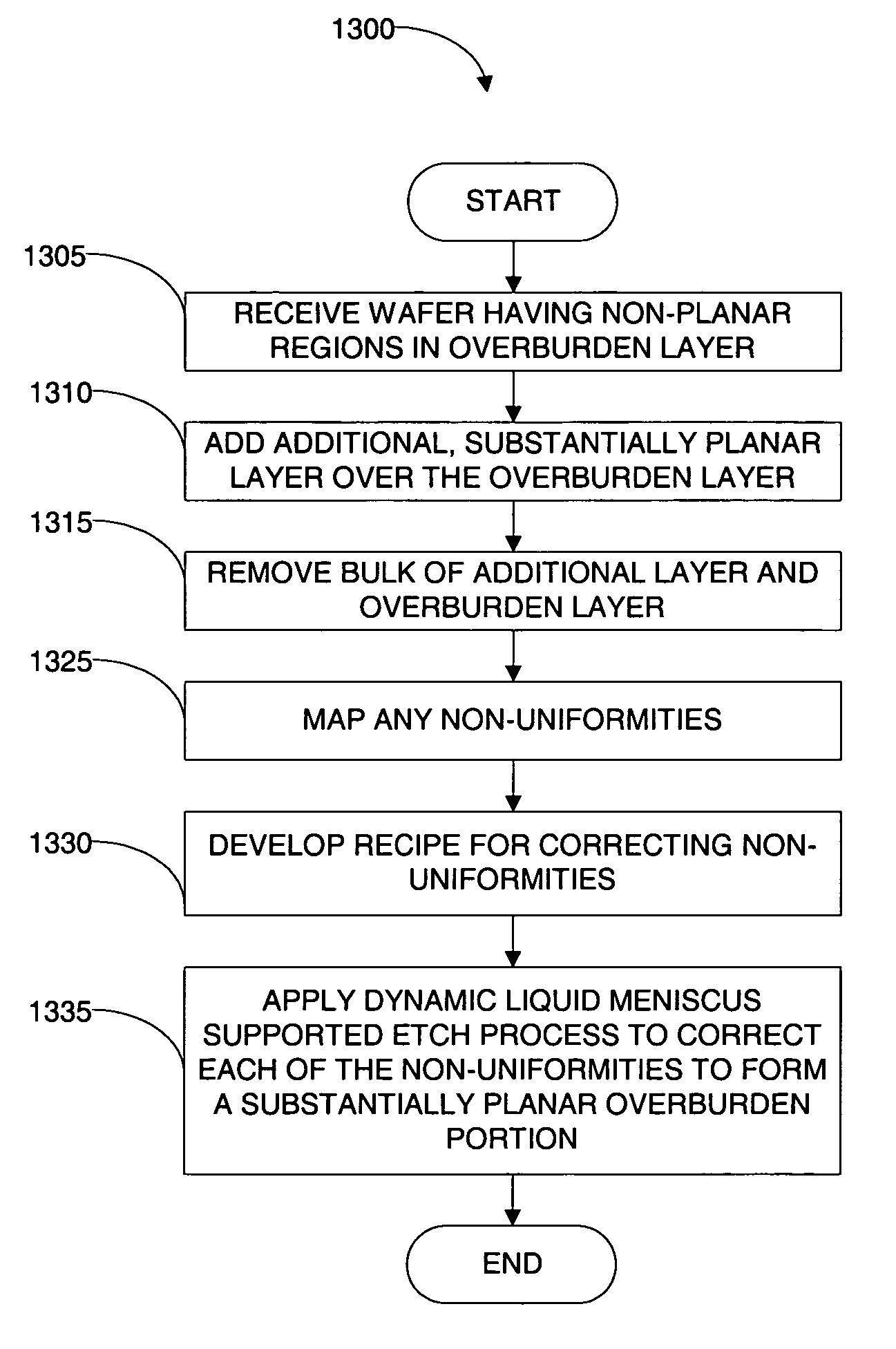
[0038]Several exemplary embodiments for an improved uniformity control and planarizing system and method will now be described. It will be apparent to those skilled in the art that the present invention may be practiced without some or all of the specific details set forth herein.

[0039]One embodiment of an improved uniformity control and planarizing system and method provides improved local planarization and uniformity across a local portion of a semiconductor substrate. The improved local planarization and uniformity substantially eliminates local nonuniformities caused by features in underlying layers and variations in deposition and etch processes. Another embodiment provides improved global planarization and uniformity across the entire substrate (e.g., edge uniformity as compared to center uniformity).

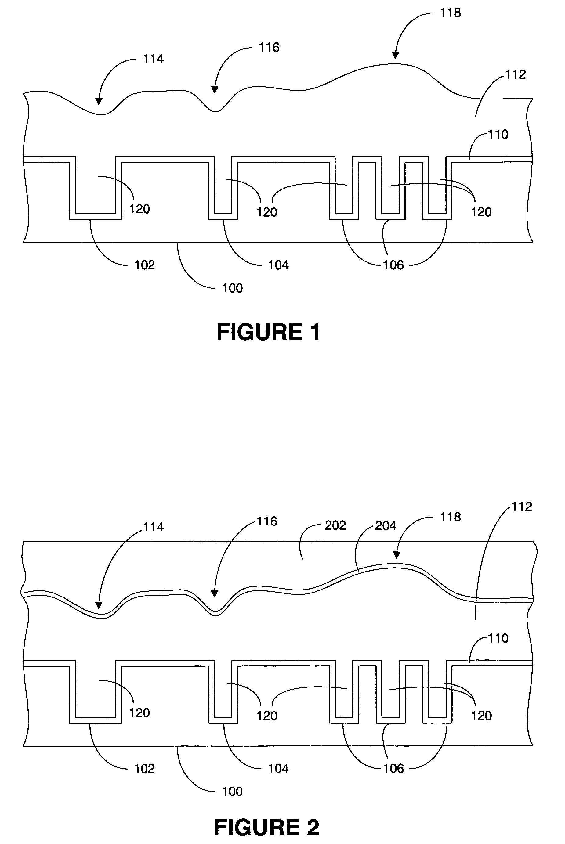
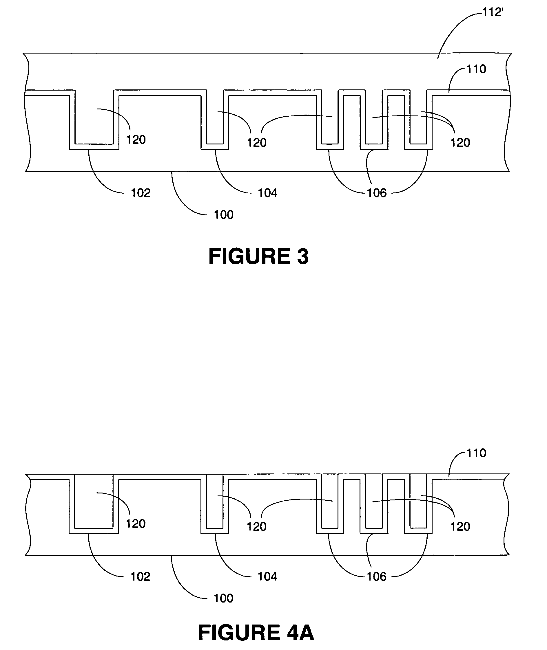
[0040]One embodiment includes a method for planarizing a patterned semiconductor substrate includes receiving a patterned semiconductor substrate. The patterned semiconductor subs...


PUM


Abstract

A system and method for planarizing and controlling non-uniformity on a patterned semiconductor substrate includes receiving a patterned semiconductor substrate. The patterned semiconductor substrate having a conductive interconnect material filling multiple features in the pattern. The conductive interconnect material having an overburden portion. A bulk of the overburden portion is removed and a remaining portion of the overburden portion has a non-uniformity. The non-uniformity is mapped, optimal solution determined and a dynamic liquid meniscus etch process recipe is developed to correct the non-uniformity. A dynamic liquid meniscus etch process, using the dynamic liquid meniscus etch process recipe, is applied to correct the non-uniformity to substantially planarize the remaining portion of the overburden portion.

Description

CROSS REFERENCE TO RELATED APPLICATIONS[0001]This application is a continuation-in-part of U.S. patent application Ser. No. 10 / 390,117, now U.S. Pat. No. 6,939,796 filed on Mar. 14, 2003 and entitled “System, Method and Apparatus For Improved Global Dual-Damascene Planarization,” which is incorporated herein by reference in its entirety. This application is also a continuation-in-part of U.S. patent application Ser. No. 10 / 390,520, now U.S. Pat. No. 6,821,899 filed on Mar. 14, 2003 and entitled “System, Method and Apparatus For Improved Local Dual-Damascene Planarization,” which is incorporated herein by reference in its entirety.BACKGROUND OF THE INVENTION[0002]1. Field of the Invention[0003]The present invention relates generally to dual damascene semiconductor manufacturing processes, and more particularly, to methods and systems for planarizing features and layers and controlling uniformity in a semiconductor manufacturing process.[0004]2. Description of the Related Art[0005]Dua...

Claims


Application Information

Patent Timeline
18 Jul 2006
Publication
US7078344B2
IPC
H01L21/302; H01J37/32; H01L21/00; H01L21/321; H01L21/3213; H01L21/44; H01L21/461; H01L21/4763; H01L21/768; H01L23/48; H01L23/52; H01L29/24; H01L29/40; H01L33/00
CPC
H01J37/32522; H01L21/32115; H01L21/32136; H01L21/7684; H01L21/67051; H01L21/6708; H01L21/67253; H01L21/67034
Inventors
BAILEY, III, ANDREW D.; RAVKIN, MICHAEL