Chip on board package for imager

a technology of imager and chip, applied in the field of chip packages, can solve the problems of inhibiting the minimization of these problems, affecting the efficiency of imagers, and causing interference between neighboring devices, and achieve the effect of reducing electrical interferen

Inactive Publication Date: 2006-07-18
RE SECURED NETWORKS LLC +1
View PDF2 Cites 26 Cited by
  • Summary
  • Abstract
  • Description
  • Claims
  • Application Information

AI Technical Summary

Benefits of technology

[0024]The chip may allow different types of signals to be input or output. The chip may operate with analog electrical signals, digital electrical signals, or some combination. In the case where the array type arrangement is used, the analog signals or the high speed digital signals may be coupled to the leads nearest the imager chip (the innermost lead layer), in order to minimize electrical interference based on the signal or on the geometries of the interconnects.

Problems solved by technology

Thus, when a high-speed digital or analog line is close to another electrical line, high switching speeds or frequencies can create interference between the neighboring due to parasitic capacitance or inductance.
The limited geometries of typical chip carrier packages inhibit the minimization of these problems.
Such problems are compounded with imager packaging.
For example, as the resolution of CMOS (Complementary Metal Oxide Semiconductor) imager sensor cores increase, attempting to successfully design and package such imagers becomes increasingly difficult due to the corresponding increase in sensitivity to parasitic capacitance and inductance inherent in the package.
Since this operation is performed before any of the devices are mounted to the module, the sealing temperatures are only limited by the properties of the case and the pins, and can be much higher than for module sealing.
This multi-stage process is expensive, cumbersome and subject to failure.
Additionally, the process of constructing a package contains many steps and uses relatively expensive materials.

Method used


Image

  • Chip on board package for imager
  • Chip on board package for imager
  • Chip on board package for imager

Examples


Embodiment Construction

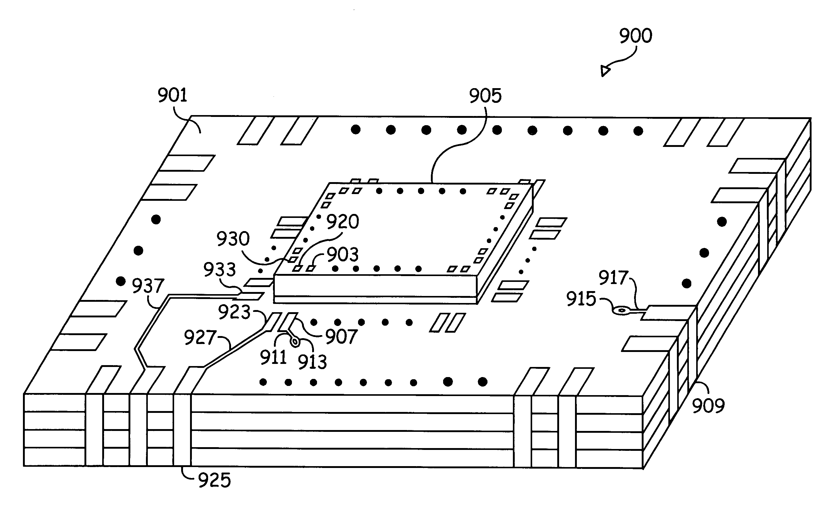
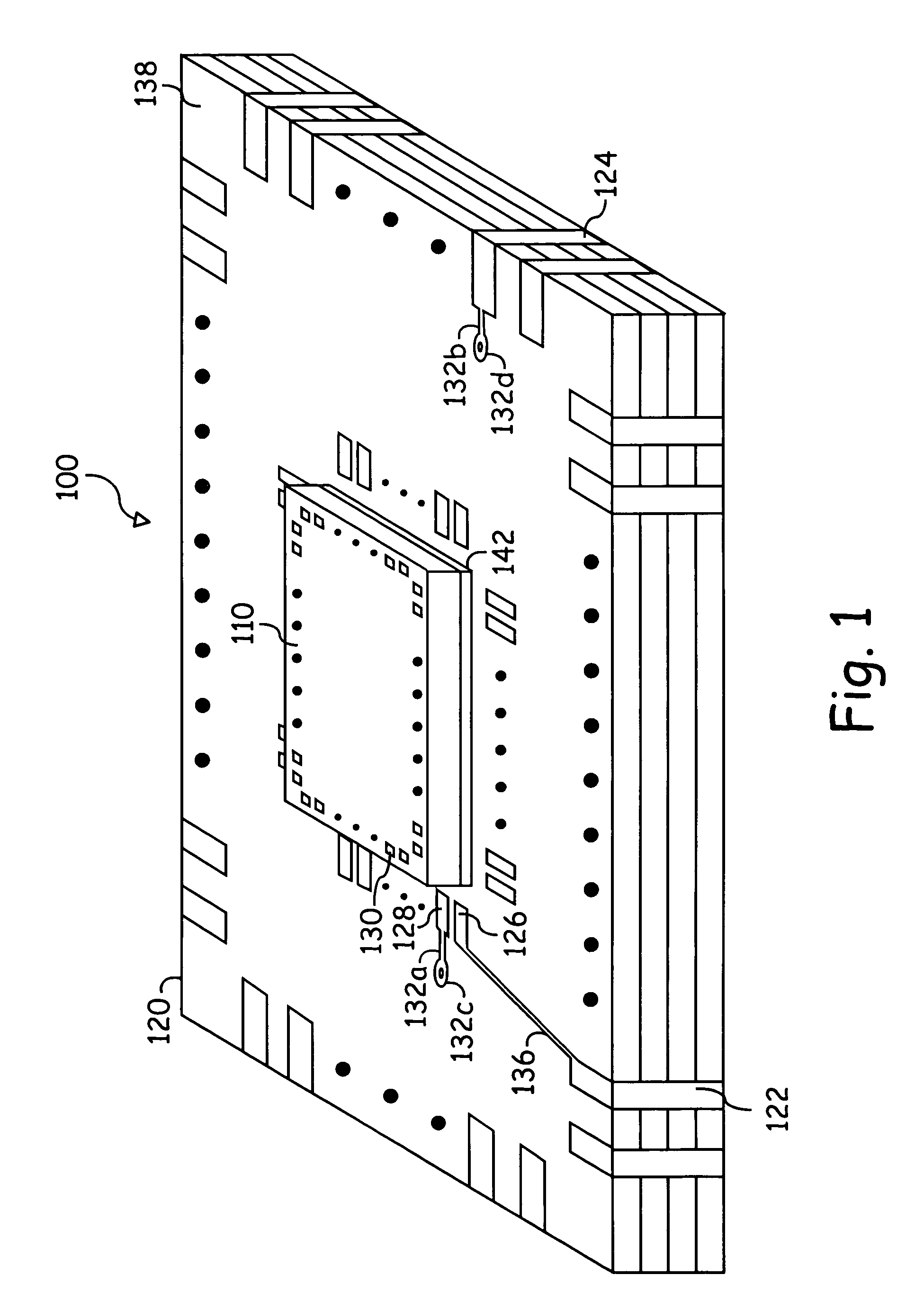
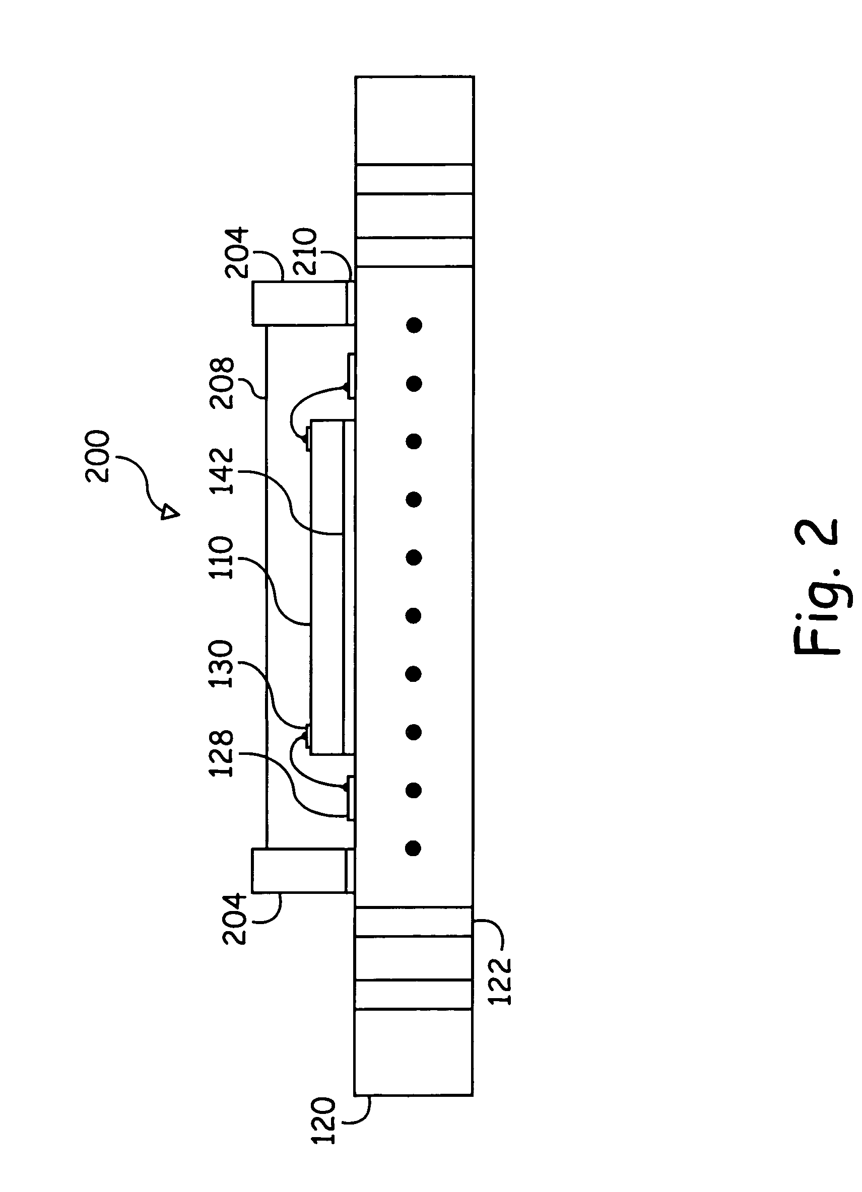
[0036]FIG. 1 is a perspective diagram of one embodiment of an imager integrated circuit package, where a printed circuit board is used in the packaging of an imager integrated circuit chip to form a leadless chip carrier type package. Specifically, an imager IC (Integrated Circuit) package 100 comprises a PCB (Printed Circuit Board) 120 and an imager IC chip 110 mounted thereon. The PCB 120 is made of any material common to the construction of any conventional PCB, or any other type of easily and mass-produced electronic component substrate.

[0037]The PCB 120 has a plurality of package leads, e.g., package leads 122 and 124. The package leads, in turn, connect to one or more electrical interconnects (such as electrical interconnects 132 and 136) within or on a surface 138 of the PCB 120. The electrical interconnects of the PCB 120 are coupled to bond leads, e.g., bond leads 126 and 128, on the surface of the PCB 120.

[0038]The imager IC chip 110 has a plurality of bond pads, e.g., bon...


PUM


Abstract

A semiconductor imager chip is mated directly to a laminate-type substrate, such as a printed circuit board. A well is formed by placing a retaining wall on the printed circuit board around the imager chip. An optical material such as a clear polymer is injected into the well to cover the imager chip. After the clear polymer cures (hardens) the retaining wall may be removed. The optical material may also have light filtering or other optical properties in addition to transmissivity. The printed circuit board may have one or more layers. Some of such layers may comprise a ground-plane. High speed digital and analog lines may be strategically routed on the one or more layers to minimize interference with adjacent signal lines. Traditional sockets that receive ceramic or plastic chip carrier packages may be used in embodiments to receive the resultant printed circuit board based chip carrier. The circuit board may comprise a typical multi-component PCB or a chip-on-board carrier design.

Description

BACKGROUND OF THE INVENTION[0001]1. Technical Field[0002]The present invention is related to chip packages for integrated circuits. More precisely, the invention is related to a chip package to alleviate wiring effects and reducing cost in a hybrid analog / digital IC chip, or a combination low speed digital / high speed digital IC chip, such as a CMOS (Complementary Metal Oxide Semiconductor) Imager.[0003]2. Related Art[0004]Conventional chip packages are made with a number of techniques. First, one type of popular chip carrier is one known as a ceramic-leaded chip carrier (CLCC). Other types of chip packages include a plastic leadless chip carrier (PLCC), multi-layer ceramic pin grid ray (PGA) package, and ball grid ray (BGA) type packages. The PLCC and CLCC packages typically contain leads at the edge of the carrier. Most imagers, for example, utilize PLCC and CLCC packaging. The PGA and BGA packages typically contain leads on the bottom of the carrier in an array pattern.[0005]In al...

Claims


Application Information

Patent Timeline
Patent Type & Authority Patents(United States)
IPC IPC(8): H01L23/02
CPCH01L27/14618H01L27/14621H01L27/14625H01L2224/16H01L2224/32225H01L2224/45144H01L2224/48227H01L2224/48472H01L2224/73265H01L2224/48091H01L2924/00014H01L2924/00
Inventor TINDLE, GARY D.GUNAWAN, FERRY
Owner RE SECURED NETWORKS LLC
Why Eureka
Try Eureka