

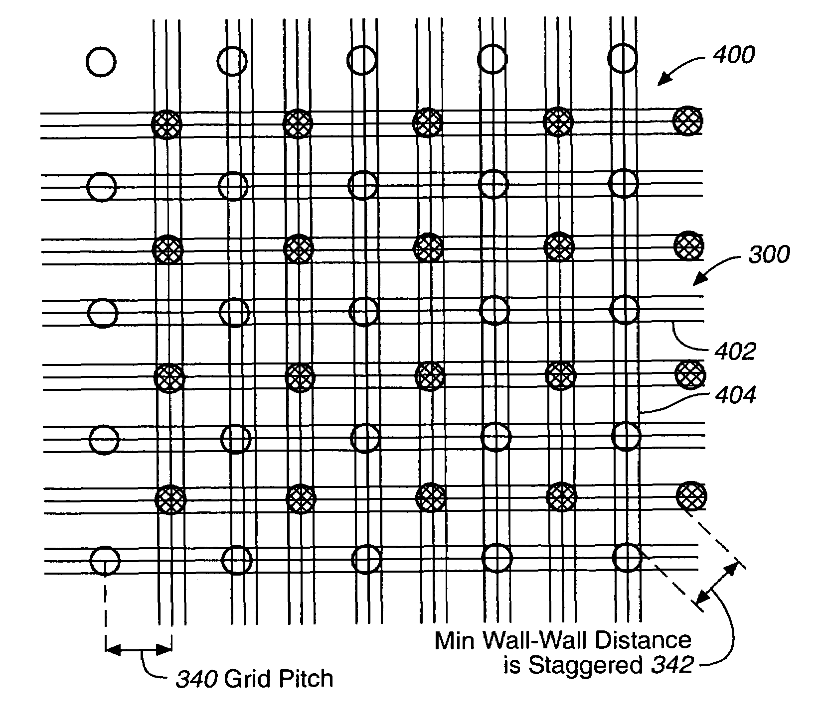
Substrate via layout to improve bias humidity testing reliability
a technology of substrate vias and humidity testing, applied in the field of integrated circuits, can solve the problems of failure in the field or during reliability testing, it is not practical to attempt to bond such tightly packed bumps to the motherboard, and the wall-to-wall distance between power and ground vias can be small
- Summary
- Abstract
- Description
- Claims
- Application Information
AI Technical Summary
Problems solved by technology
Method used
Image

Examples
Embodiment Construction
[0024]This disclosure relates to a core voltage via grid pattern for substrates used in various packaging technologies in integrated circuits, such as flip chip packages, wire bond packages, printed circuit board applications and the like.
[0025]The disclosure, including the figures, describes substrates in the context of ball grid arrays and ball assignment schemes among others, with reference to several illustrative examples. Other examples are contemplated and are mentioned below or are otherwise imaginable to someone skilled in the art. The scope of the invention is not limited to the few examples, i.e., the described embodiments of the invention. Rather, the scope of the invention is defined by reference to the appended claims. Changes can be made to the examples, including alternative designs not disclosed and to other packaging or substrate applications, and still be within the scope of the claims.
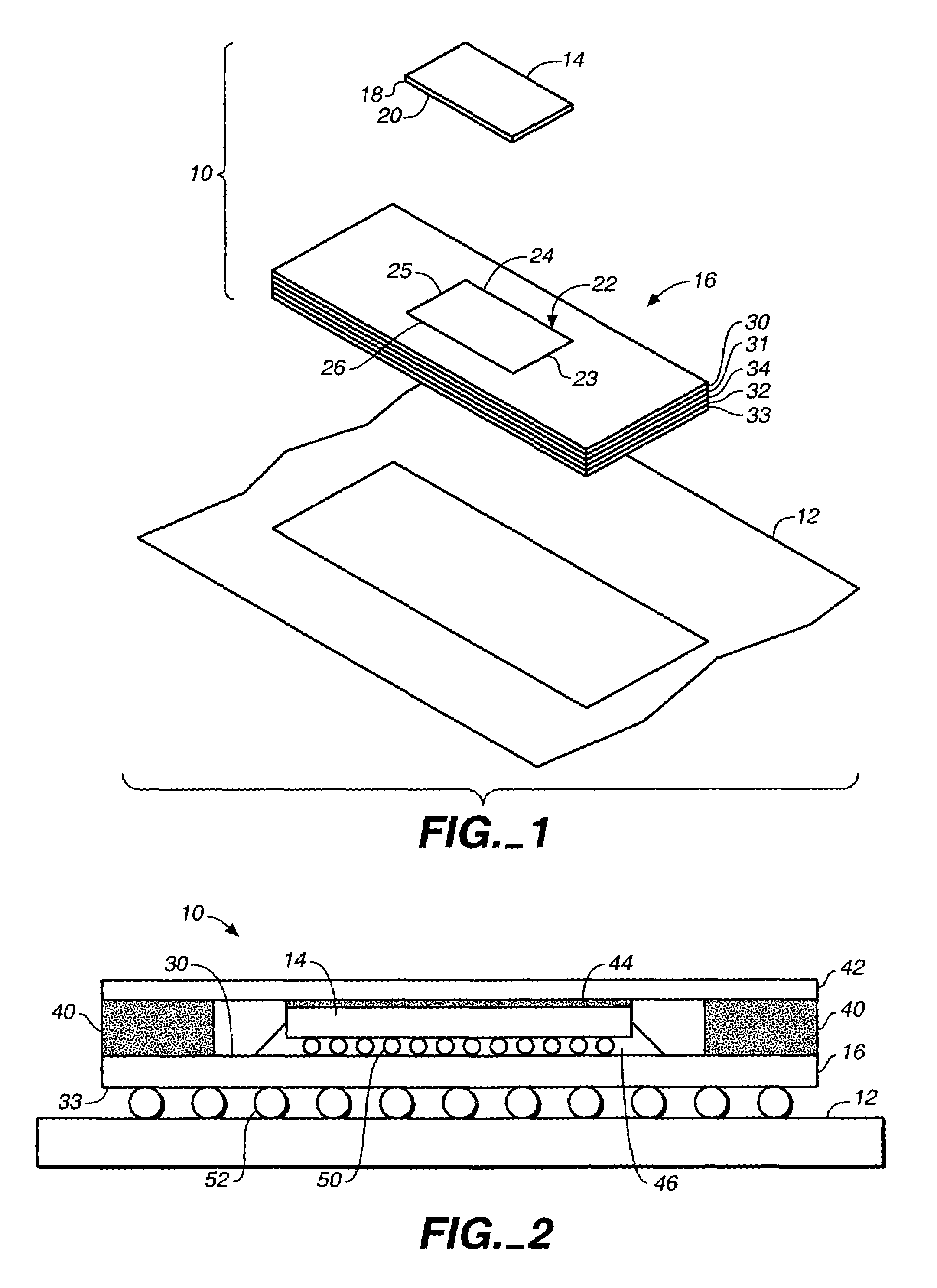
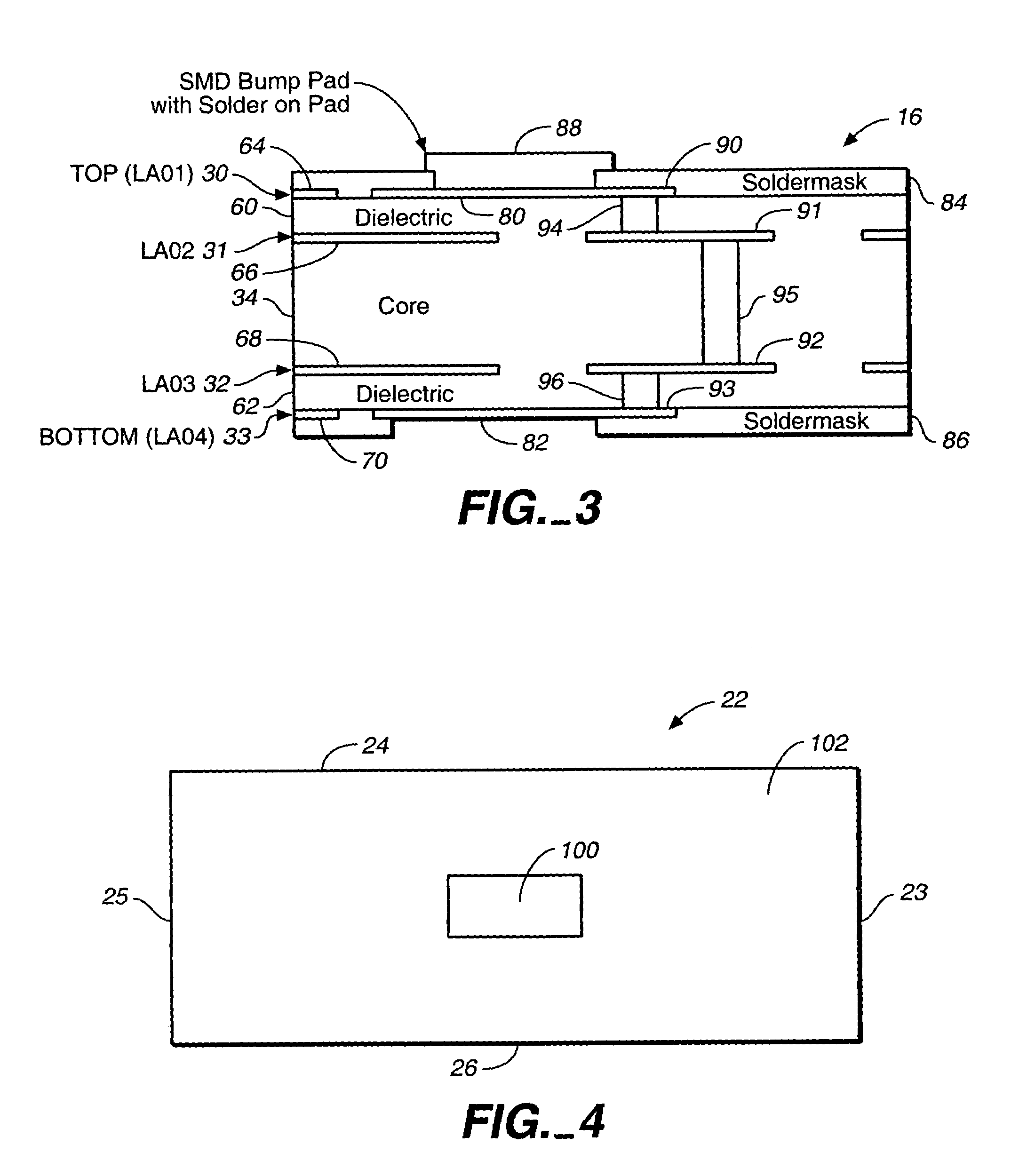
[0026]FIG. 1 is an exploded, perspective view of a flip chip 10, which can be mo...
PUM
| Property | Measurement | Unit |
|---|---|---|
| Polarity | aaaaa | aaaaa |
| Electric potential / voltage | aaaaa | aaaaa |
| Area | aaaaa | aaaaa |
Abstract
Description
Claims
Application Information