Printed built-in antenna for use in a portable electronic communication apparatus

a portable electronic communication and built-in antenna technology, which is applied in the structural form of the antenna, the structure of the antenna, and the antenna earthing, etc., can solve the problems of affecting the performance of the antenna, the connector and the assembling of the antenna and the pcb add considerable cost to the mobile telephone, and the antenna is still too large to fit the small mobile telephone chassis, etc., to achieve the effect of maximizing the interior space of the electronic communication apparatus, good radiation characteristics, and low cos

Inactive Publication Date: 2006-07-25
SONY ERICSSON MOBILE COMM AB
View PDF18 Cites 42 Cited by
  • Summary
  • Abstract
  • Description
  • Claims
  • Application Information

AI Technical Summary

Benefits of technology

[0008]It is an object of the present invention to provide a built-in antenna having a printed pattern of conductive material with good radiation characteristics in at least one frequency band, which is inexpensive to manufacture and utilizes the interior space of an electronic communication apparatus effectively. More specifically, it is an object of the invention to provide an antenna, which can be connected to the RF circuits of the printed circuit board (PCB) of the apparatus without any conventional connectors, such as pogo-pins. A further object of the invention is to eliminate the mechanical tolerances involved with the assembly of the antenna and the PCB.
[0011]The above objects are also achieved by a portable electronic communication apparatus comprising a PCB having RF circuits connected to an built-in antenna, which is printed on the PCB of the apparatus and connected to the RF circuits. Also, the apparatus of the invention comprises an extended ground plane, which provides good radiation characteristics for the antenna.
[0012]By providing the inventive antenna manufacturing costs of the portable electronic communication apparatus is lowered and the interior space of the apparatus is utilized more effectively.
[0013]As an alternative, the antenna pattern can be provided to form a multi-port antenna comprising antenna arms having four connections to the circuitry of the PCB. In this embodiment the cost savings in relation the known art will be even bigger. Also, as no connectors, such as pogo-pins are needed, the insertion loss is lowered. Further, by providing separate antenna patterns for the Rx and Tx circuits respectively, it is possible to connect the antenna to the Rx and Tx circuitry respectively, without having an antenna switch, which will lower the cost of the mobile phone even more.

Problems solved by technology

As the mobile telephones becomes smaller and smaller, both conventional microstrip patch and PIFA antennas are still too large to fit small mobile telephone chassis.
This is particularly problematic when the new generation of mobile telephones needs multiple antennas for cellular, wireless local are network, GPS and diversity.
Disadvantages of built-in antennas known in the art are that both the connectors and the assembling of the antenna and the PCB add considerable cost to the mobile telephone.
Also, the mechanical tolerances involved in the assembling of the conventional built-in antenna and the PCB effect the performance of the antenna negatively.
That is, it is difficult to obtain exactly the same position of the antenna in relation to the signal source, and sufficient connection of the pogo-pins.
Also, in antenna configurations known in the art, the space between the antenna and the PCB is not utilized effectively, by e.g. positioning electronic components in between them.
Further, as it becomes more and more common with multi-port antennas in portable electronic communication apparatuses, i.e. antennas having separate antenna arms for each Rx (receiver unit) and Tx (transmitter unit), the number of connectors is increasing and consequently the cost and the problem with mechanical tolerances.

Method used


Image

  • Printed built-in antenna for use in a portable electronic communication apparatus
  • Printed built-in antenna for use in a portable electronic communication apparatus
  • Printed built-in antenna for use in a portable electronic communication apparatus

Examples


Embodiment Construction

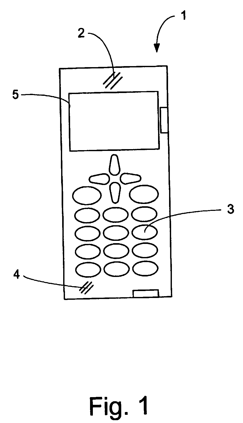
[0021]FIG. 1 illustrates a mobile telephone 1 as one example in which the printed built-in antenna according to the invention may be used. However, the inventive antenna may be used in virtually any other portable electronic communication apparatus, in which a built-in antenna is preferred.

[0022]The mobile telephone 1 shown in FIG. 1 comprises a loudspeaker 2, a keypad 3, a microphone 4, and a display 5 as is generally known in the art. Further, the mobile telephone 1 comprises the antenna according to the invention, which is built-in into the chassis of the mobile telephone 1.

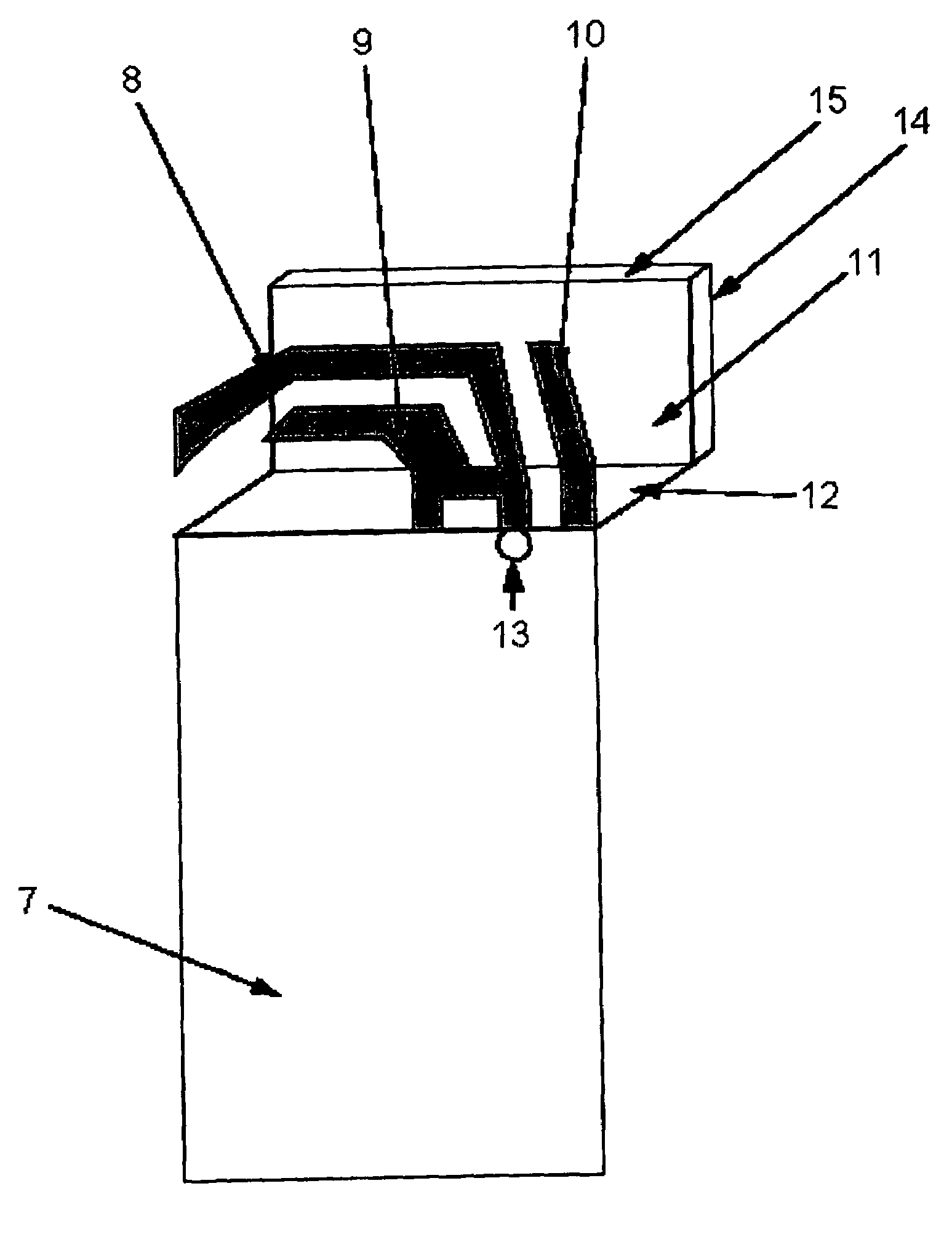
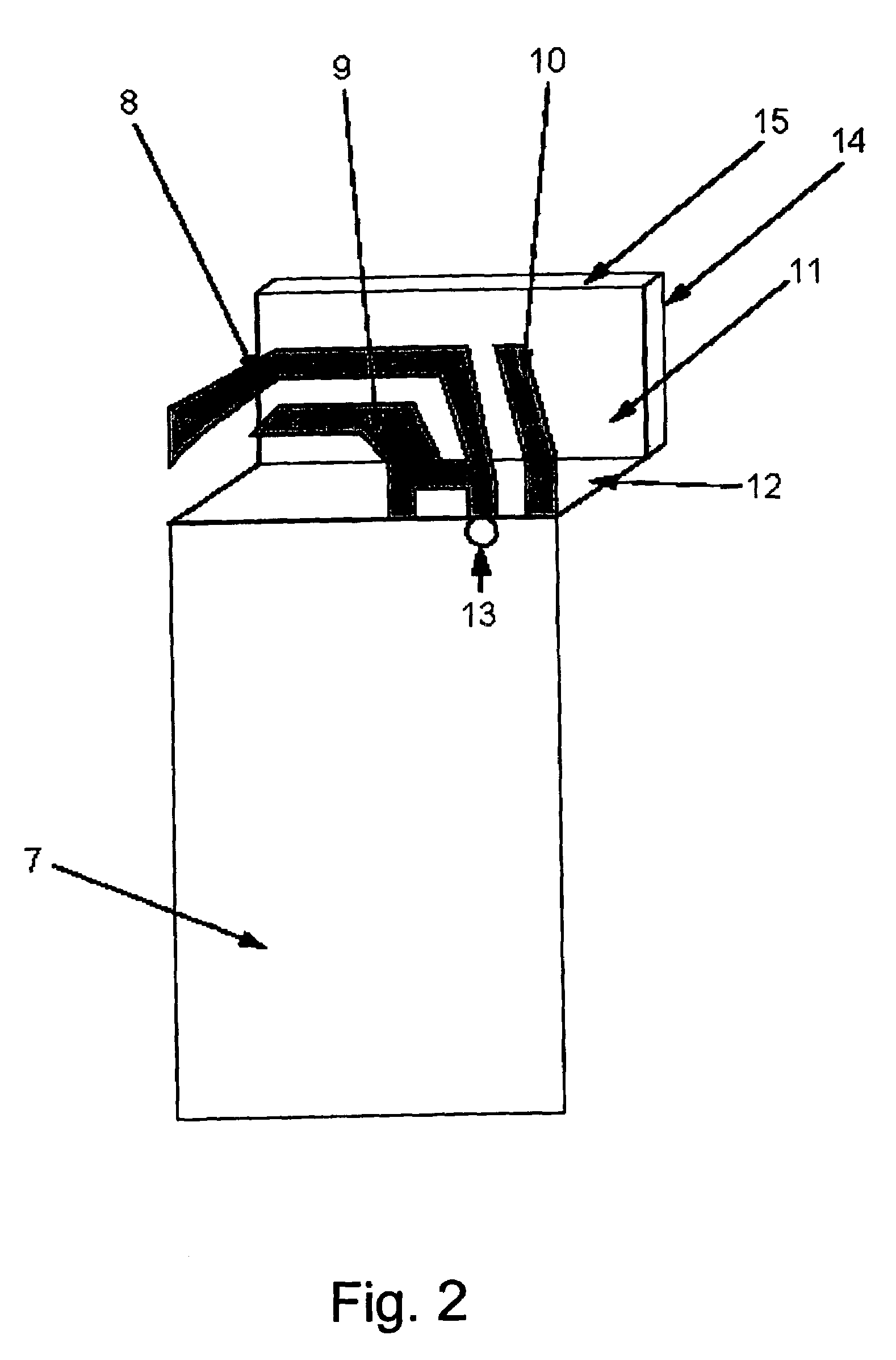
[0023]FIG. 2 illustrates a multi-band printed built-in antenna according to a first embodiment of the invention. The antenna comprises a pattern of conductive material printed directly on the main printed circuit board (PCB) 7 of the mobile telephone 1. In FIG. 2, the PCB 7 is shown as ending at the beginning of the antenna pattern. However, as is apparent to the man skilled in the art, this is only for illust...


PUM


Abstract

An antenna for use in a portable electronic communication apparatus has a pattern of a conductive material. The pattern of conductive material is printed on the Printed Circuit Board (PCB) (7), comprising the RF circuitry of the portable electronic communication apparatus, to which antenna pattern is connected. The pattern comprises a first and second antenna arm, which together for a PIFA antenna and are resonating in a first and second frequency band, respectively. As an alternative, the antenna pattern forms a multi-port antenna having separate antenna arms for Rx and Tx, respectively.

Description

RELATED APPLICATIONS[0001]The present application is a 35 U.S.C. §371 national phase application of PCT International Application No. PCT / EP03 / 04298, having an international filing date of Apr. 25, 2003 and claiming priority to European Patent Application No. 02009863.8, filed May 2, 2002, and to U.S. Provisional Application No. 60 / 379,138 filed May 9, 2002, the disclosures of which are incorporated herein by reference in their entireties. The above PCT International Application was published in the English language and has International Publication No. WO 03 / 094289 A1.TECHNICAL FIELD[0002]The invention relates to an antenna for use in a portable electronic communication apparatus such as a mobile telephone. More specifically, the invention relates to a built-in antenna comprising a pattern of conductive material, which is printed on the printed circuit board (PCB) of the portable electronic communication apparatus. The invention also relates to a portable electronic communication a...

Claims


Application Information

Patent Timeline
Patent Type & Authority Patents(United States)
IPC IPC(8): H01Q1/24H01Q5/00H01Q5/371H01Q5/378H01Q5/40H01Q9/04H01Q19/00
CPCH01Q1/243H01Q9/0421H01Q5/40H01Q5/371H01Q5/378H01Q19/005
Inventor YING, ZHINONGHAKANSSON, KENNETH
Owner SONY ERICSSON MOBILE COMM AB
Why Eureka
Try Eureka