Serial peripheral interface (SPI) apparatus with write buffer for improving data throughput

a peripheral interface and buffer technology, applied in the field of serial peripheral interfaces, can solve the problems of reducing the data throughput of the system, wasting time and sacrificing data throughput, and generating write collision errors, so as to improve data throughput, simplify the monitoring function of the software driver, and avoid stretching the master clock

Active Publication Date: 2006-07-25
ATMEL CORP
View PDF10 Cites 29 Cited by
  • Summary
  • Abstract
  • Description
  • Claims
  • Application Information

AI Technical Summary

Benefits of technology

[0010]Accordingly, this object of the invention is achieved by a serial peripheral interface apparatus that uses a second parallel write buffer to enable a control processing unit (CPU) to load in a subsequent data byte while a current data byte is being transferred serially from a first write buffer through the apparatus. The serial peripheral interface with two parallel write buffers does not have to wait for the previous data byte to complete the serial transfer and other control commands to avoid data collision and the transfer of a subsequent data byte. The second parallel write buffer releases the burden for the software driver, since the software driver does not have to monitor a master-slave register for the completion of a current data byte transmission before loading a subsequent byte for transmission without data collision. Thus, a state machine and a second write buffer are at the gate level and effectively simplify the monitoring function of the software driver by providing an early “load enable” signal to the software driver.
[0011]The subsequent data byte is transferred into the second parallel write buffer only after a finite state machine controller examines two signals: the status of the primary write buffer and the status of the second parallel write buffer. Afterwards, the state machine controller orders the subsequent data byte to be transferred from the second parallel write buffer into the primary write buffer when the load enable is favorable and the write buffer is available. The load enable is favorable for the second write buffer when a bit counter counts the first half of the serial transfer of the previous data byte (which occupies the primary write buffer) instead of waiting for the complete serial transfer and other control commands. Thus, the second parallel write buffer avoids stretching the master clock and inherently improves data throughput without using complex and costly external devices.

Problems solved by technology

Because this write corrupts any transfer in progress, a write-collision error is generated.
The write collision avoidance in the Motorola SPI causes a degradation in the data throughput.
The software driver is not located at each local SPI, and therefore it takes time and sacrifices in the data throughput of the system.
One problem inherent to such circuitry requires the software driver to wait for a current data byte transmission to complete and for other necessary control commands in order to avoid write collision.

Method used


Image

  • Serial peripheral interface (SPI) apparatus with write buffer for improving data throughput
  • Serial peripheral interface (SPI) apparatus with write buffer for improving data throughput
  • Serial peripheral interface (SPI) apparatus with write buffer for improving data throughput

Examples


Embodiment Construction

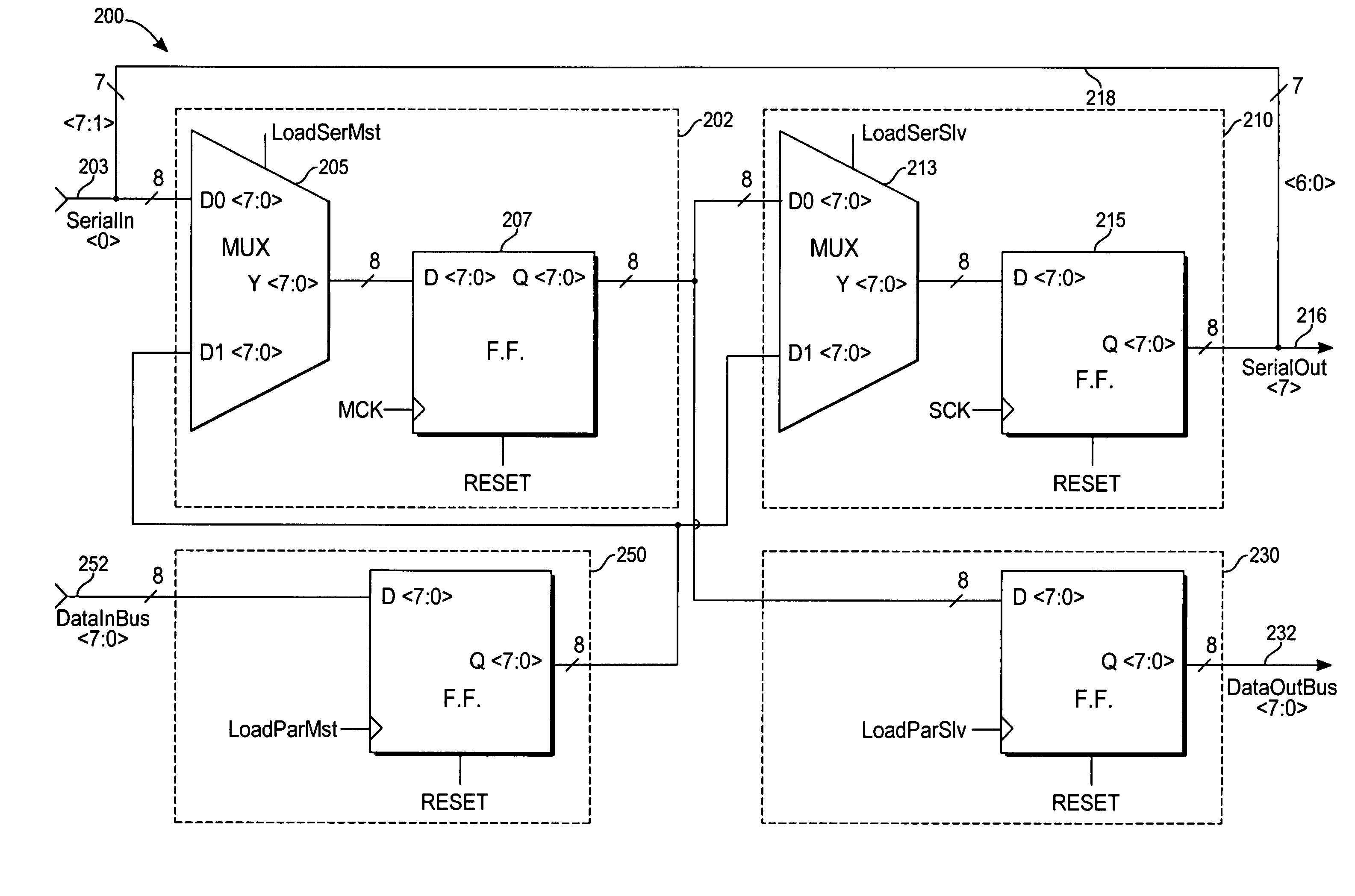
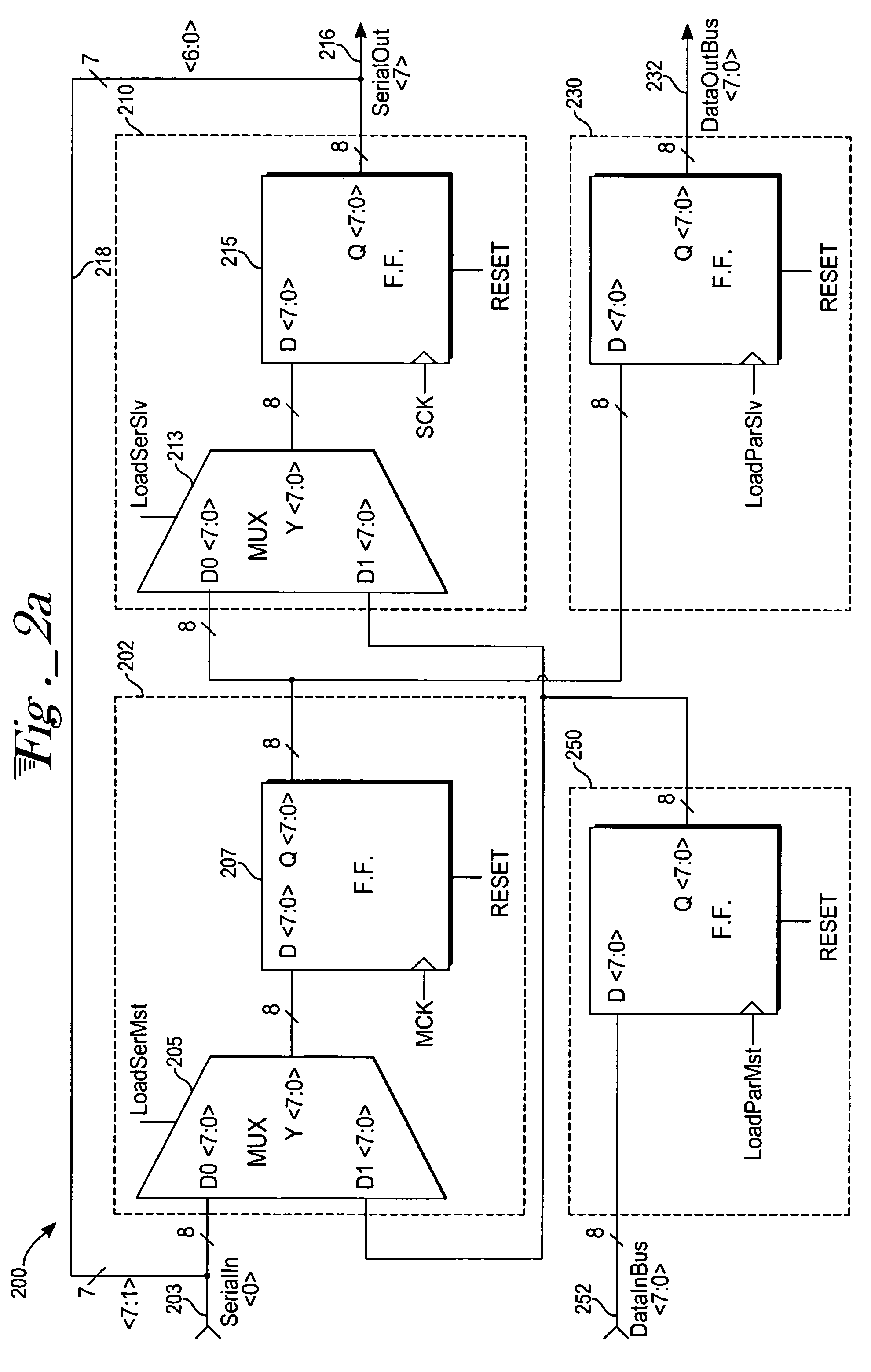
[0018]With reference to FIG. 2A, an exemplary embodiment of the new enhanced mode SPI 200 block diagram contains a new register latch serving as a second parallel write buffer 250. Its purpose is to accept the content of input data on the parallel input data bus DataInBus 252 and store it while a previous data byte is still being transmitted. The enhanced SPI 200 comprises a serial master register 202, a serial slave register 210, a parallel slave register 230, and the second parallel write buffer 250.

[0019]The serial registers 202 and 210 are coupled together for transferring data serially through a serial output SerialOut 216. (Data can also be received serially through a serial input SerialIn 203 and converted by the serial registers into a parallel output for the bus DataOutBus 232.) The output of the master register 202 is coupled to the input of the slave register 210, while the output of the slave register 210 is coupled to both the serial output SerialOut 216 and a feedback ...


PUM


Abstract

A serial peripheral interface apparatus has a second parallel write buffer to load in a subsequent data byte while a current data byte is being transferred serially through the apparatus instead of waiting for the previous data byte to complete the serial transfer and other commands to avoid write collision. The subsequent data byte is transferred into the second parallel write buffer only after the software driven CPU examines the status of a load enable and the status of a write buffer provided by a finite state machine controller. The software driven CPU orders the subsequent data byte to be transferred into the second parallel write buffer when the load enable is favorable and the second parallel write buffer is available. The load enable becomes favorable when a bit counter counts the first half of the transfer of the previous data set. Thus, the second parallel write buffer avoids the stretching the master clock and improves data throughput of the system.

Description

TECHNICAL FIELD[0001]This invention relates generally to a serial peripheral interface. More specifically, this invention relates to write collision avoidance for improving data throughput of a serial peripheral interface.BACKGROUND ART[0002]The serial peripheral interface (SPI) is one of two independent serial communications subsystems included on the Motorola MC68HC11A8 microcontroller. As the name implies, the SPI is primarily used to allow a microcontroller unit (MCU) to communicate with peripheral devices. The central element in the Motorola serial peripheral interface system is a block containing the shift register and the read data buffer. The system is single buffered in the transmit direction and double buffered in the receive direction. This fact means that a subsequent data byte for transmission cannot be written to the shifter until the current data byte transmission is complete; however, received data is transferred into a parallel read data buffer so the shifter is fre...

Claims


Application Information

Patent Timeline
Patent Type & Authority Patents(United States)
IPC IPC(8): G06F3/00G06F13/12G06F13/00G06F13/40
CPCG06F13/4054
Inventor LAMBRACHE, EMILFROEMMING, BENJAMIN F.
Owner ATMEL CORP
Why Eureka
Try Eureka