

RF current return path for a large area substrate plasma reactor
a plasma reactor and large area technology, applied in the direction of electrical equipment, basic electric elements, electric discharge tubes, etc., can solve the problems of contaminating the substrate, affecting the processing environment, and less effective for large area glass substrate processing applications
- Summary
- Abstract
- Description
- Claims
- Application Information
AI Technical Summary
Benefits of technology
Problems solved by technology
Method used
Image

Examples
Embodiment Construction
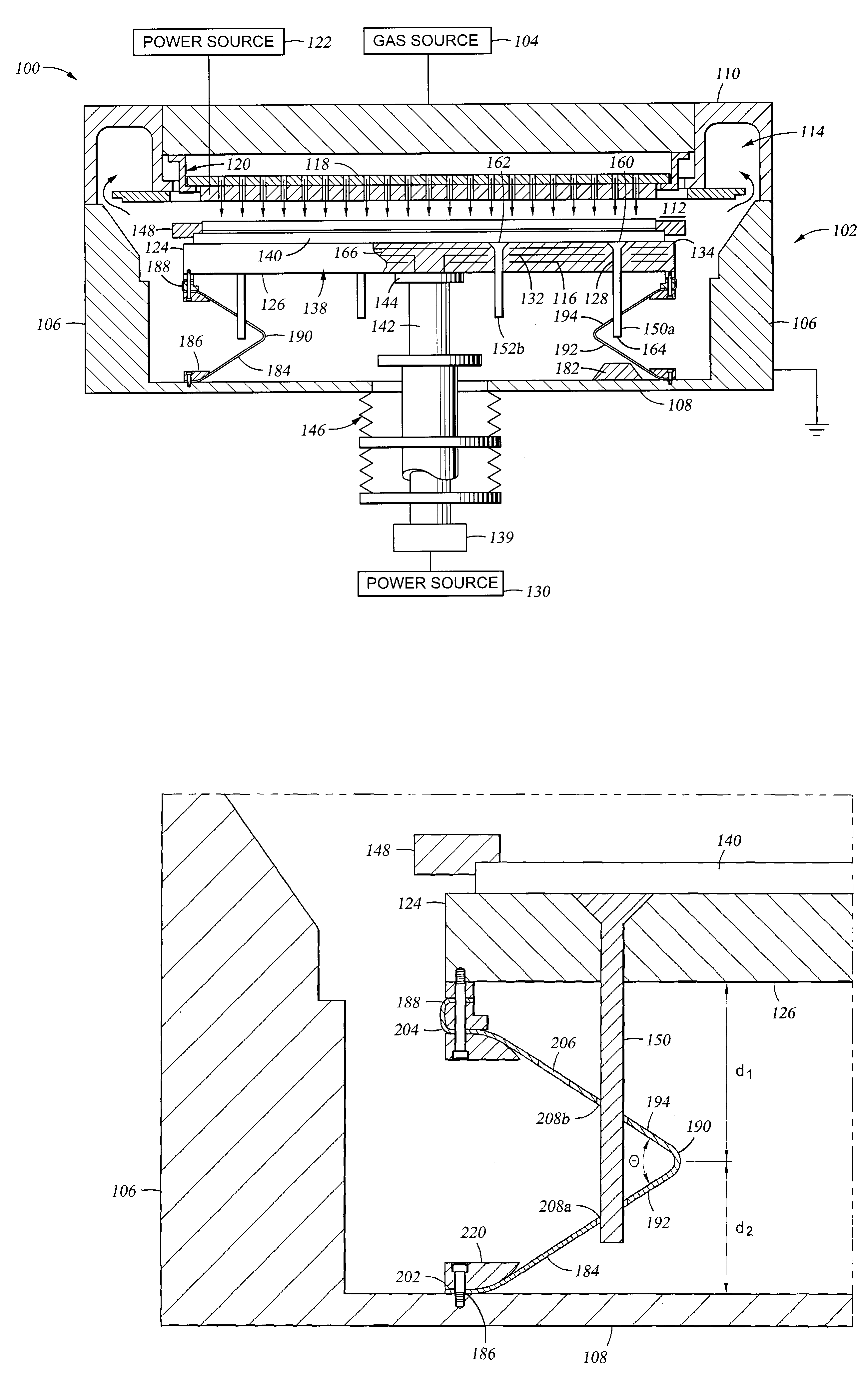
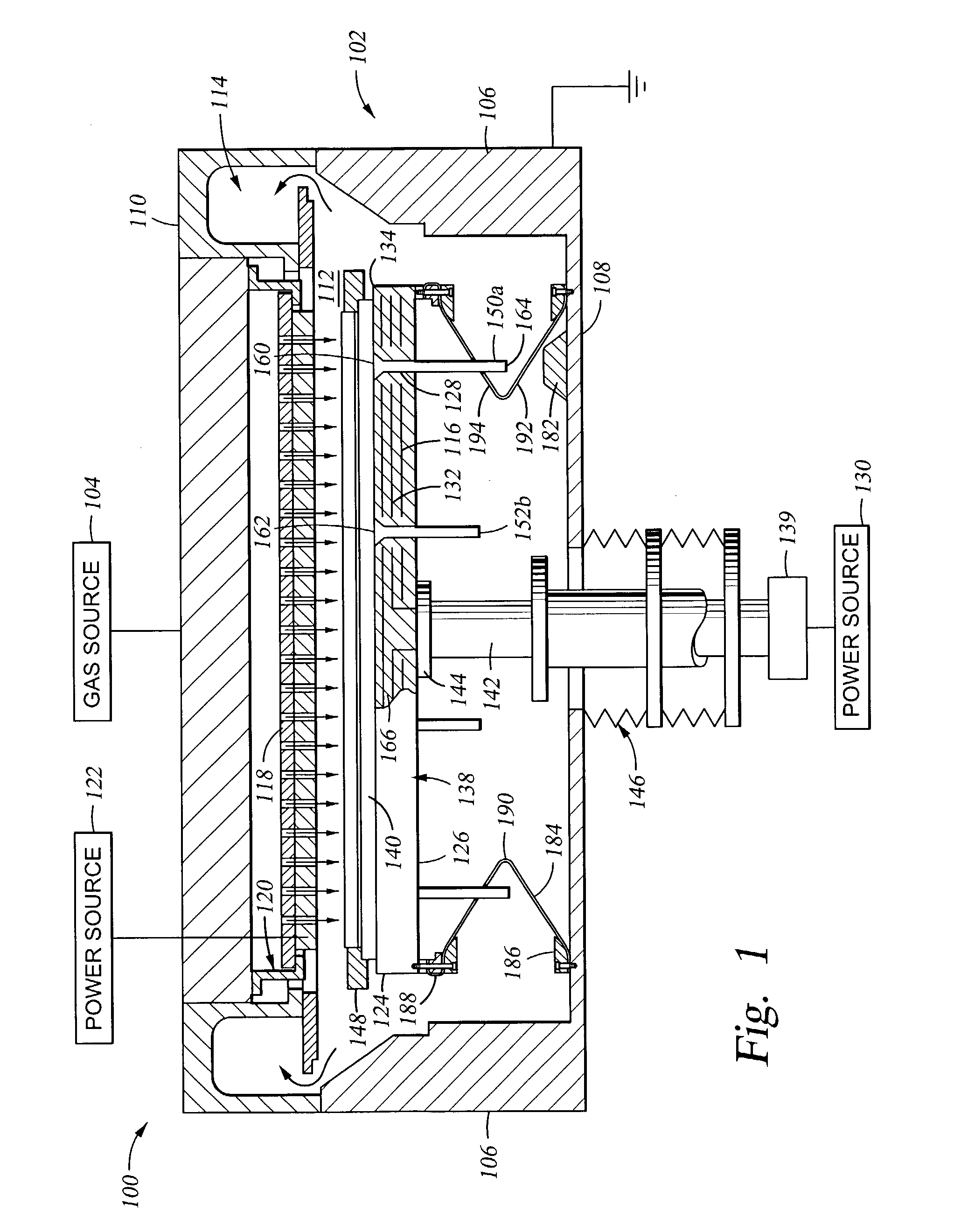
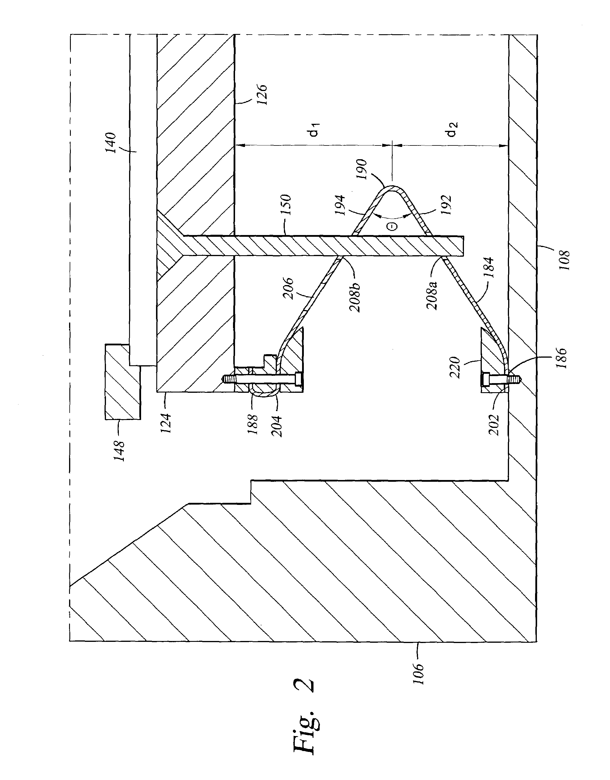
[0024]The invention generally provides an RF current return path for systems supporting large area substrates. The invention is illustratively described below in reference to a plasma enhanced chemical vapor deposition (PECVD) system, such as those commercially available from AKT, a division of Applied Materials, Inc. of Santa Clara, Calif. However, it should be understood that the invention has utility in other system configurations such as physical vapor deposition systems, etch systems and other processing systems in which providing a low-impedance RF current return path between a substrate support and a chamber housing the substrate support is desired.
[0025]FIG. 1 is a cross sectional view of one embodiment of a plasma enhanced chemical vapor deposition system 100 having one embodiment of a ground curtain 184 that provides a low-impedance path between a substrate support assembly 138 and ground. The system 100 generally includes a grounded chamber 102 coupled to a gas source 104...
PUM
| Property | Measurement | Unit |
|---|---|---|
| temperature | aaaaa | aaaaa |
| size | aaaaa | aaaaa |
| temperature | aaaaa | aaaaa |
Abstract
Description
Claims
Application Information