Semiconductor package with reduced inductive coupling between adjacent bondwire arrays

a technology of inductive coupling and semiconductor package, which is applied in the direction of semiconductor devices, semiconductor/solid-state device details, amplifiers with semiconductor devices/discharge tubes, etc., can solve the problems of adverse perturbation of the performance of a doherty power amplifier, the unique challenges of semiconductor package design, and the worsening of power efficiency as output power decreases

Active Publication Date: 2011-10-04
NXP USA INC
View PDF6 Cites 27 Cited by
  • Summary
  • Abstract
  • Description
  • Claims
  • Application Information

AI Technical Summary

Problems solved by technology

However, power efficiency worsens as output power decreases.
However, it presents unique challenges in terms of semiconductor package design.
That is, the performance of a Doherty power amplifier can be adversely perturbed by coupling (i.e., the transfer of energy from one circuit component to another through a shared magnetic or electric field) between adjacent bondwire arrays of the corresponding components of the Doherty power amplifier.
Unfortunately, maintaining spatial distance between amplifiers, for example, the carrier and peaking amplifiers of a Doherty power amplifier, to control crosstalk caused by inductive coupling limits the miniaturization of the semiconductor package.
Limiting the miniaturization of such devices is undesirable where low cost, a low weight, and a small volume are essential for application.

Method used


Image

  • Semiconductor package with reduced inductive coupling between adjacent bondwire arrays
  • Semiconductor package with reduced inductive coupling between adjacent bondwire arrays
  • Semiconductor package with reduced inductive coupling between adjacent bondwire arrays

Examples


Embodiment Construction

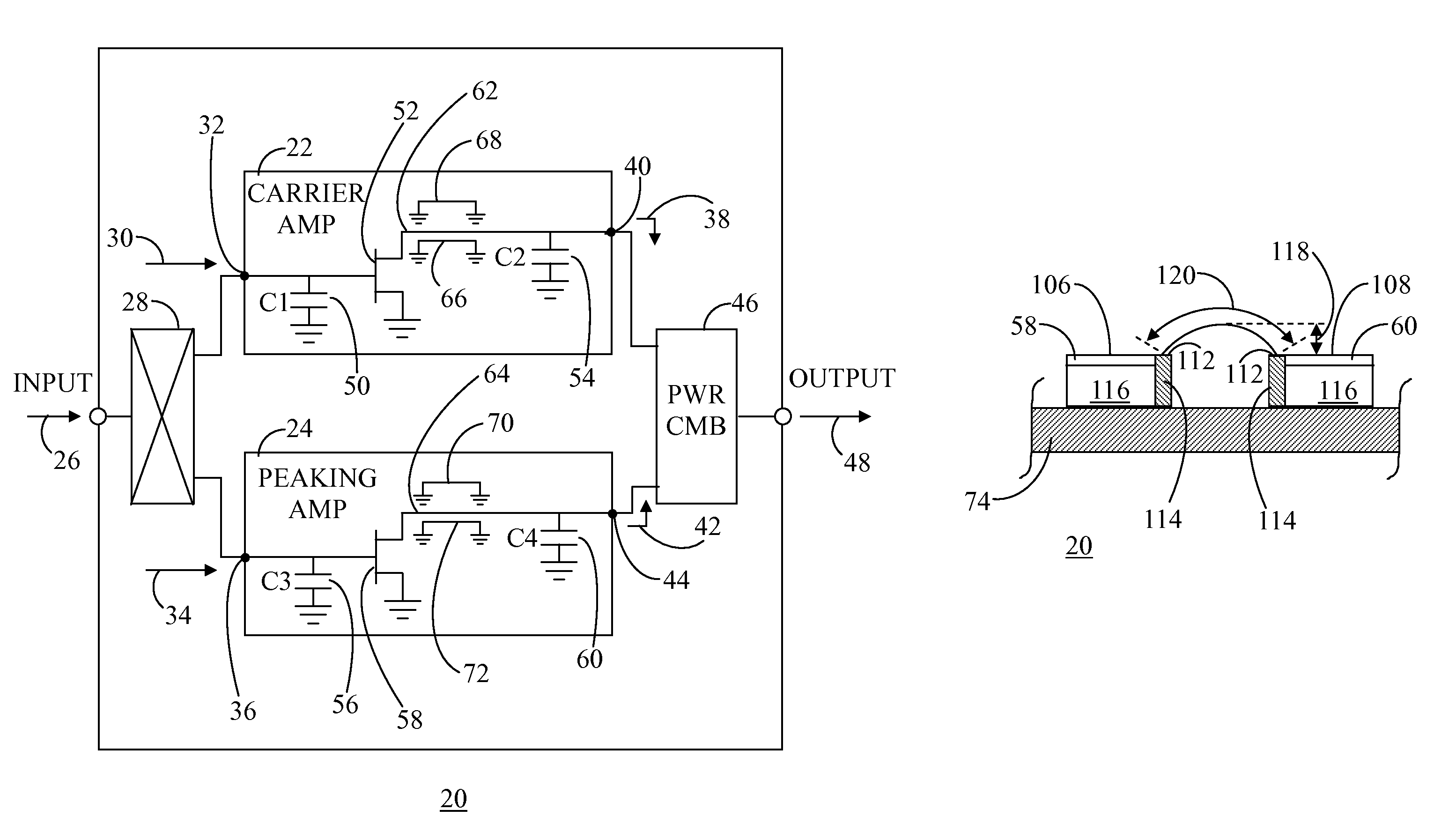
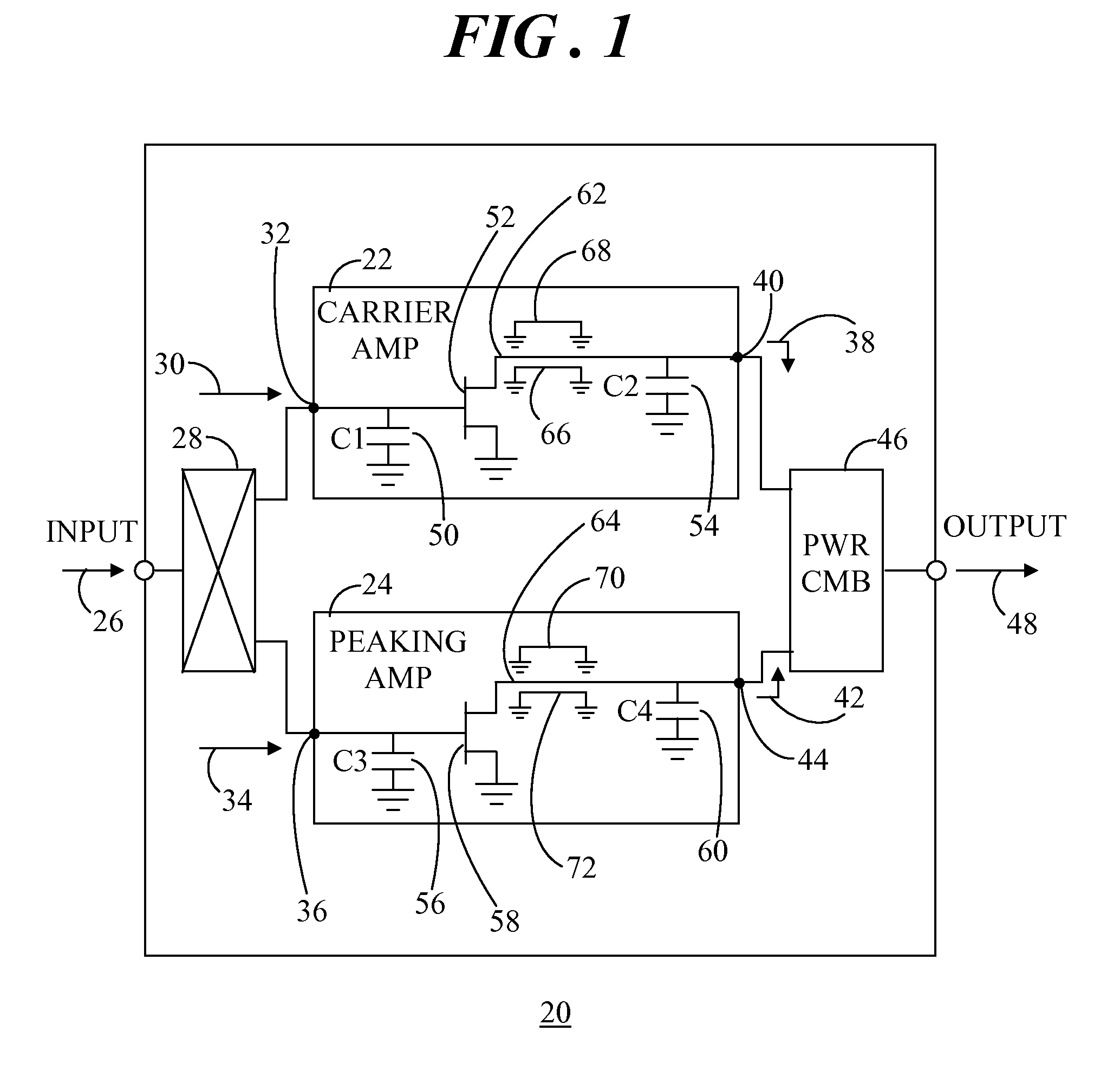
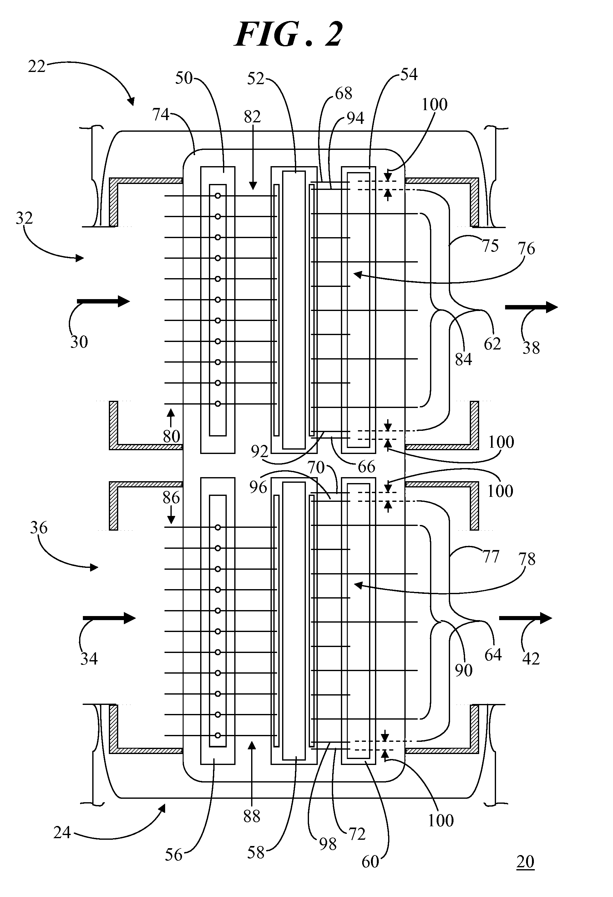
[0013]An embodiment entails a high power Doherty amplifier semiconductor package with compact design. In particular, techniques are employed for reducing inductive coupling so that the carrier and peaking amplifiers of a Doherty power amplifier may be implemented in a single package, referred to herein as a dual-path semiconductor package. This enables the use of a Doherty power amplifier semiconductor package in base station power amplifiers, cell phones, blue tooth devices, and other devices dependent upon semiconductor packages, where low cost, low weight, and small volume are essential for application. An embodiment described herein reduces inductive coupling between bondwire arrays in a Doherty power amplifier. However, it will become apparent that the techniques described below for reducing inductive coupling may be implemented in a variety of semiconductor device designs.

[0014]FIG. 1 shows a block diagram of a Doherty power amplifier semiconductor package 20. Doherty power am...


PUM


Abstract

A semiconductor package (20) includes circuits (22, 24). The circuit (22) includes electrical devices (52, 54) interconnected by a bondwire array (62). Likewise, the circuit (24) includes electrical devices (58, 60) interconnected by a bondwire array (64). Signal wires (76) of the bondwire array (62) are proximate to signal wires (78) of the bondwire array (64). Ground wires (66, 68) are located on either side of, and close to, bondwire array (62). Ground wires (70, 72) are located on either side of, and close to, bondwire array (64). The ground wires (66, 68, 70,72) are electrically coupled to a ground region (74). The ground wires (66, 68, 70, 72) reduce a magnetic flux density (140) via induced return currents (126, 130) on the ground wires of opposite polarity to signal currents (124, 128) on the bondwire arrays (62, 64) to reduce inductive coupling between the adjacent bondwire arrays (62, 64).

Description

TECHNICAL FIELD OF THE INVENTION[0001]The present invention relates generally to semiconductor packages. More specifically, the present invention relates to a semiconductor package with reduced inductive coupling between adjacent bondwire arrays.BACKGROUND OF THE INVENTION[0002]Wireless communication systems often employ power amplifiers for increasing the power of a signal. In a wireless communication system, a power amplifier is usually designated as the last amplifier in a transmission chain (the output stage) and it is the amplifier stage that typically requires the most attention to power efficiency. Indeed, the performance of a transceiver in a wireless communication system depends primarily on the performance of the power amplifier. High gain, high linearity, stability, and a high level of power-added efficiency (i.e., ratio of the difference between the output power and the input power to DC power) are characteristics of an ideal amplifier.[0003]In general, a power amplifier...

Claims


Application Information

Patent Timeline
Patent Type & Authority Patents(United States)
IPC IPC(8): H01L23/52H03F3/60
CPCH01L23/66H01L24/49H03F1/0288H01L2223/6611H01L2223/6644H01L2224/48091H01L2224/48472H01L2224/49111H01L2224/49175H01L2924/01082H01L2924/14H01L2924/19041H01L2924/3011H01L2924/00014H01L24/48H01L2924/01033H01L2924/00H01L2224/48137H01L2224/85207H01L2224/45099H01L2224/05599
Inventor ROMERO, MANUEL F.AAEN, PETER H.
Owner NXP USA INC
Why Eureka
Try Eureka