Circuits with a trench capacitor having micro-roughened semiconductor surfaces

a trench capacitor and semiconductor surface technology, applied in the field of integrated circuits, can solve the problems of inability to differentiate between charges, inability to store sufficient charge of capacitors, and inability to store enough charge, etc., and achieve the effect of increasing the surface area

Inactive Publication Date:
View PDF127 Cites 81 Cited by
  • Summary
  • Abstract
  • Description
  • Claims
  • Application Information

AI Technical Summary

Problems solved by technology

Unfortunately, at some point, the capacitors become too small to store sufficient charge and sense amplifiers in the memory device are unable to differentiate between charge due to noise and the charge due to data stored in the cell.
This can lead to errors in the output of a memory device making the memory device useless in the electronic system.
First, many manufacturers use “stacked” capacitors to store data for the memory cell.
One problem with the use of stacked capacitors is their positioning above the surface of the substrate.
This positioning can interfere with the proper functioning of the equipment used to fabricate other parts of a larger circuit.
One problem with this technique is the lack of control over the distribution of the pores in the surface of the single crystalline silicon.
Thus, the '542 Patent does not provide a technique that can be used reliably for large scale production of memory devices.

Method used


Image

  • Circuits with a trench capacitor having micro-roughened semiconductor surfaces
  • Circuits with a trench capacitor having micro-roughened semiconductor surfaces
  • Circuits with a trench capacitor having micro-roughened semiconductor surfaces

Examples


Embodiment Construction

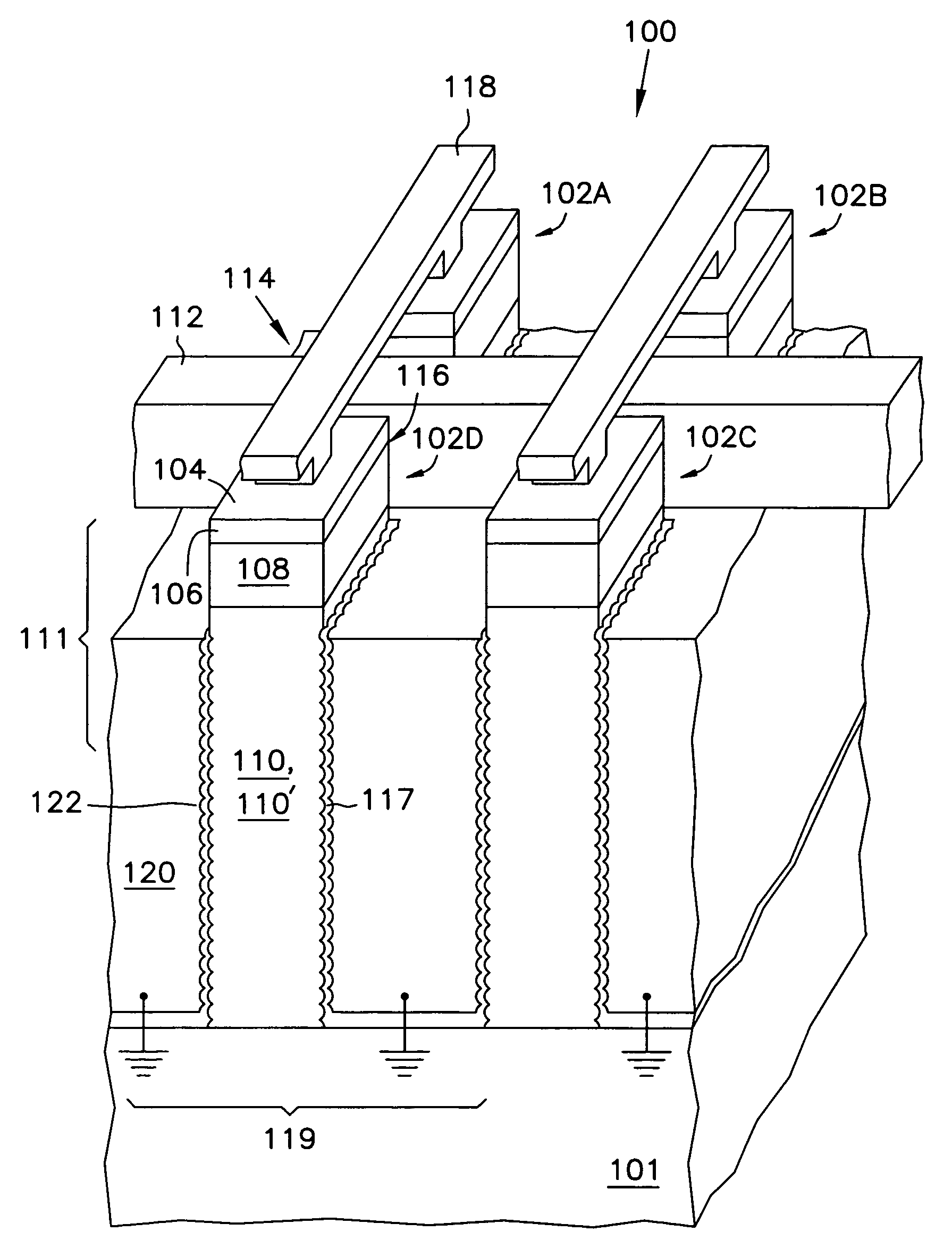
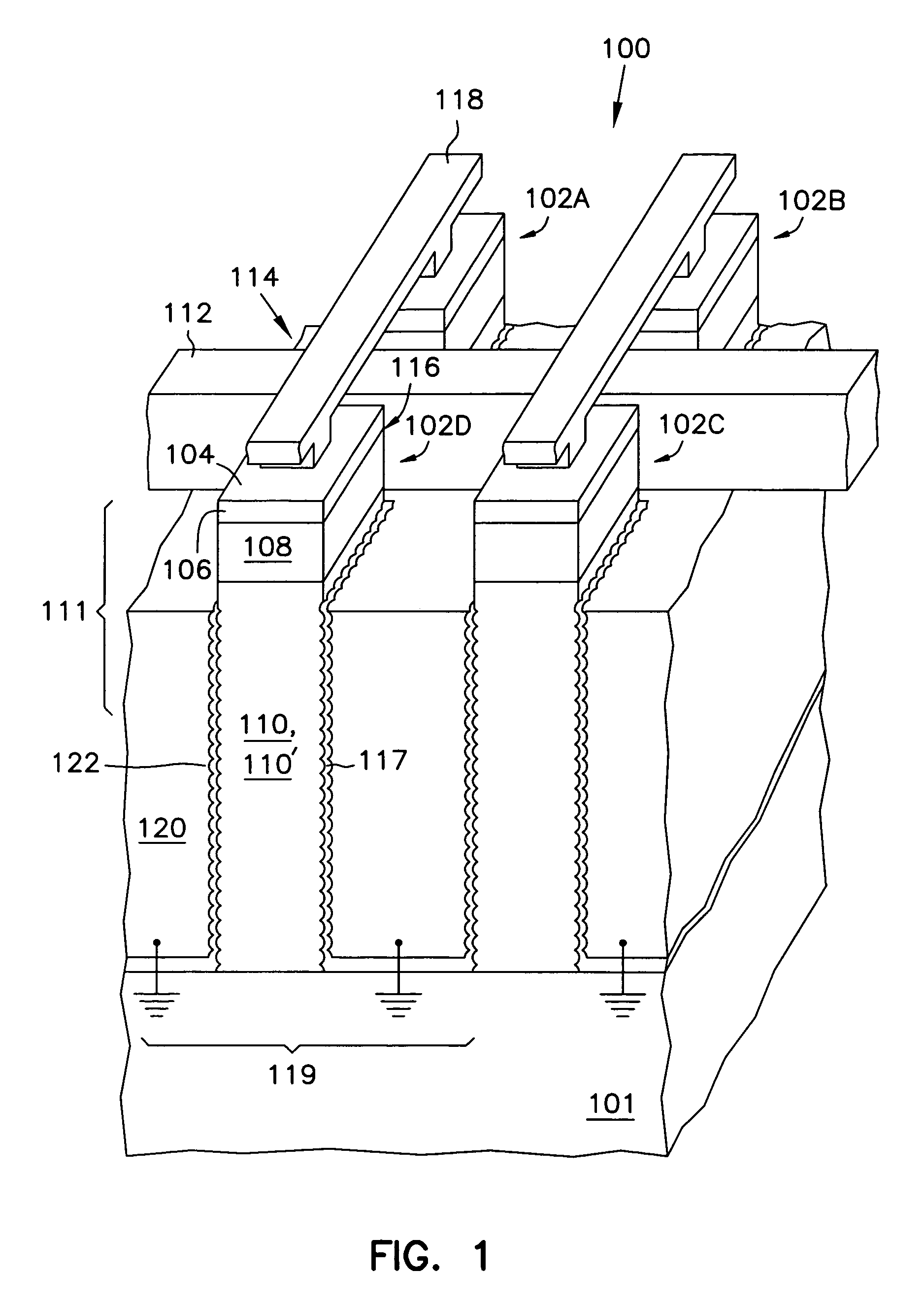
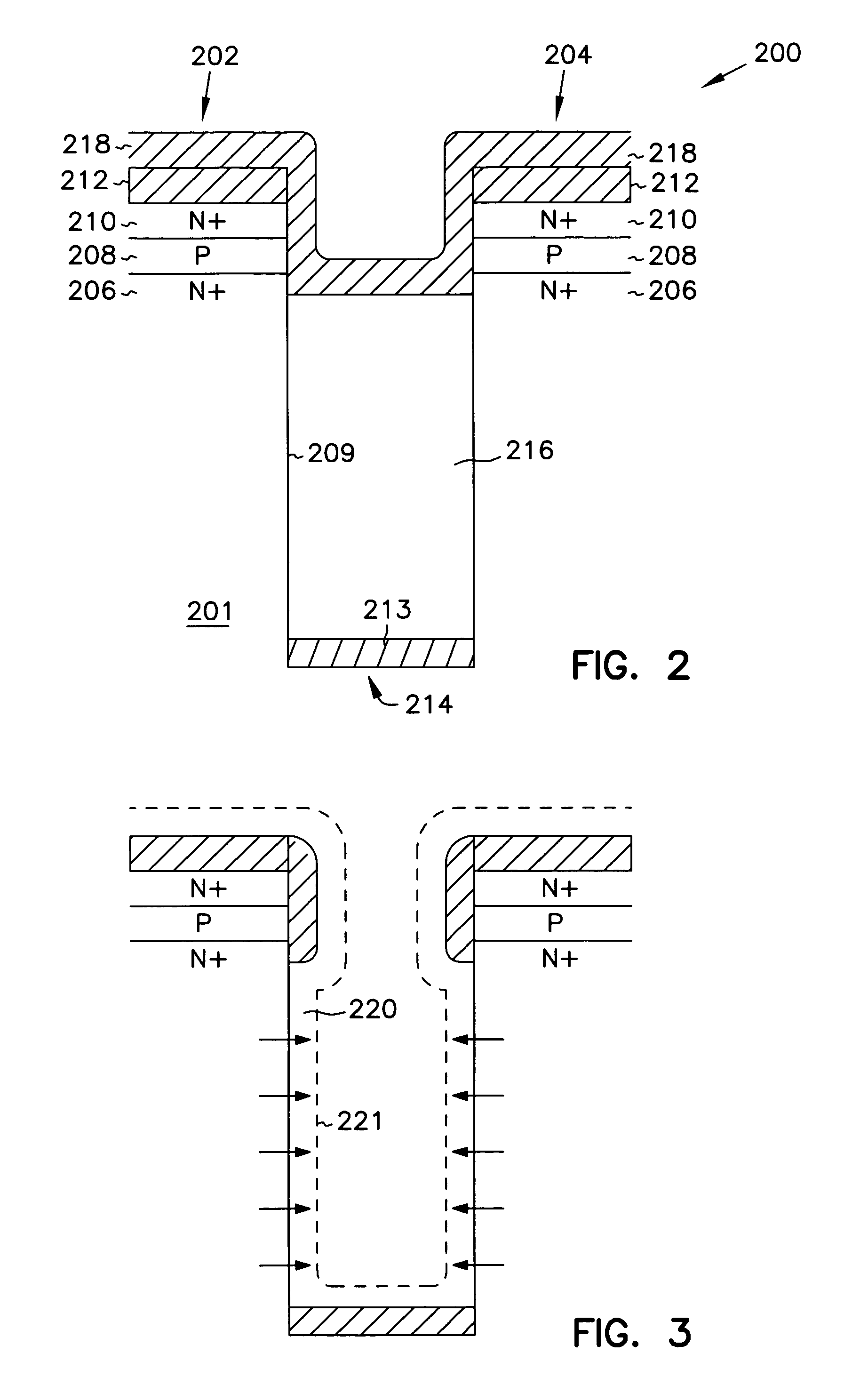
[0020]In the following detailed description of the preferred embodiments, reference is made to the accompanying drawings which form a part hereof, and in which is shown by way of illustration specific illustrative embodiments in which the invention may be practiced. These embodiments are described in sufficient detail to enable those skilled in the art to practice the invention, and it is to be understood that other embodiments may be utilized and that logical, mechanical and electrical changes may be made without departing from the spirit and scope of the present invention. The following detailed description is, therefore, not to be taken in a limiting sense.

[0021]In the following description, the terms wafer and substrate are interchangeably used to refer generally to any structure on which integrated circuits are formed, and also to such structures during various stages of integrated circuit fabrication. Both terms include doped and undoped semiconductors, epitaxial layers of a s...


PUM


Abstract

A method for forming a trench capacitor. The method includes forming a trench in a semiconductor substrate. A conformal layer of semiconductor material is deposited in the trench. The surface of the conformal layer of semiconductor material is roughened. An insulator layer is formed outwardly from the roughened, conformal layer of semiconductor material. A polycrystalline semiconductor plate is formed outwardly from the insulator layer in the trench.

Description

[0001]This application is a Divisional of U.S. application Ser. No. 09 / 010,729, filed Jan. 22, 1998, now U.S. Pat. No. 6,025,225.TECHNICAL FIELD OF THE INVENTION[0002]The present invention relates generally to the field of integrated circuits and, in particular, to circuits with a trench capacitor having micro-roughened semiconductor surfaces and methods for forming the same.BACKGROUND OF THE INVENTION[0003]Electronic systems, such as microprocessor based computers, typically operate on data that is stored in electronic form in a memory device. The memory device stores the data at specified voltage levels in an array of cells. Conventionally, the voltage levels represent that the data is either a logical “1” or a logical “0.” In dynamic random access memory (DRAM) devices, for example, the cells store the data as a charge on a capacitor. When the data is read from the memory device, sense amplifiers detect the level of charge stored on a particular capacitor so as to produce a logic...

Claims


Application Information

Patent Timeline
Patent Type & Authority Patents(United States)
IPC IPC(8): H01L27/108H01L21/02H01L21/334H01L21/8242
CPCH01L27/10861H01L29/66181H01L28/82H10B12/038
Inventor FORBES, LEONARDGEUSIC, JOSEPH E.AHN, KIE Y.
Why Eureka
Try Eureka