Semiconductor device having projected electrodes and structure for mounting the same

a technology of stress relaxation and semiconductor devices, which is applied in the direction of semiconductor devices, semiconductor/solid-state device testing/measurement, and device details. it is easy to improve the connection reliability and facilitate the inspection of the semiconductor devi

Inactive Publication Date: 2006-08-01
RENESAS TECH CORP
View PDF12 Cites 9 Cited by
  • Summary
  • Abstract
  • Description
  • Claims
  • Application Information

AI Technical Summary

Benefits of technology

[0015]Yet another object of the present invention is to provide a semiconductor device which has Pb-free solder and can improve a connection reliability.
[0016]A still further object of the present invention is to provide a method for facilitating inspection of a semiconductor device with use of a stress relaxation structure of a projected shape formed on the semiconductor device.

Problems solved by technology

For this reason, it is difficult to efficiently relax a stress applied to the respective external connection terminals with use of the stress relaxation layer.
In a semiconductor device having the multiplicity of external connection terminals, thus, it becomes more difficult to make the device small in size and to increase the number of such pins.
When the stress relaxation layer contains a filler, further, the stress relaxation layer has a rough surface and thus it is hard to form a fine wiring on the surface of the stress relaxation layer.
Further, the aforementioned second to fourth known examples have a problem that, since the entire projection playing a role in relaxing a stress is entirely covered with the metallic layer or the like, the stress relaxing function of the projection is reduced.

Method used


Image

  • Semiconductor device having projected electrodes and structure for mounting the same
  • Semiconductor device having projected electrodes and structure for mounting the same
  • Semiconductor device having projected electrodes and structure for mounting the same

Examples


Embodiment Construction

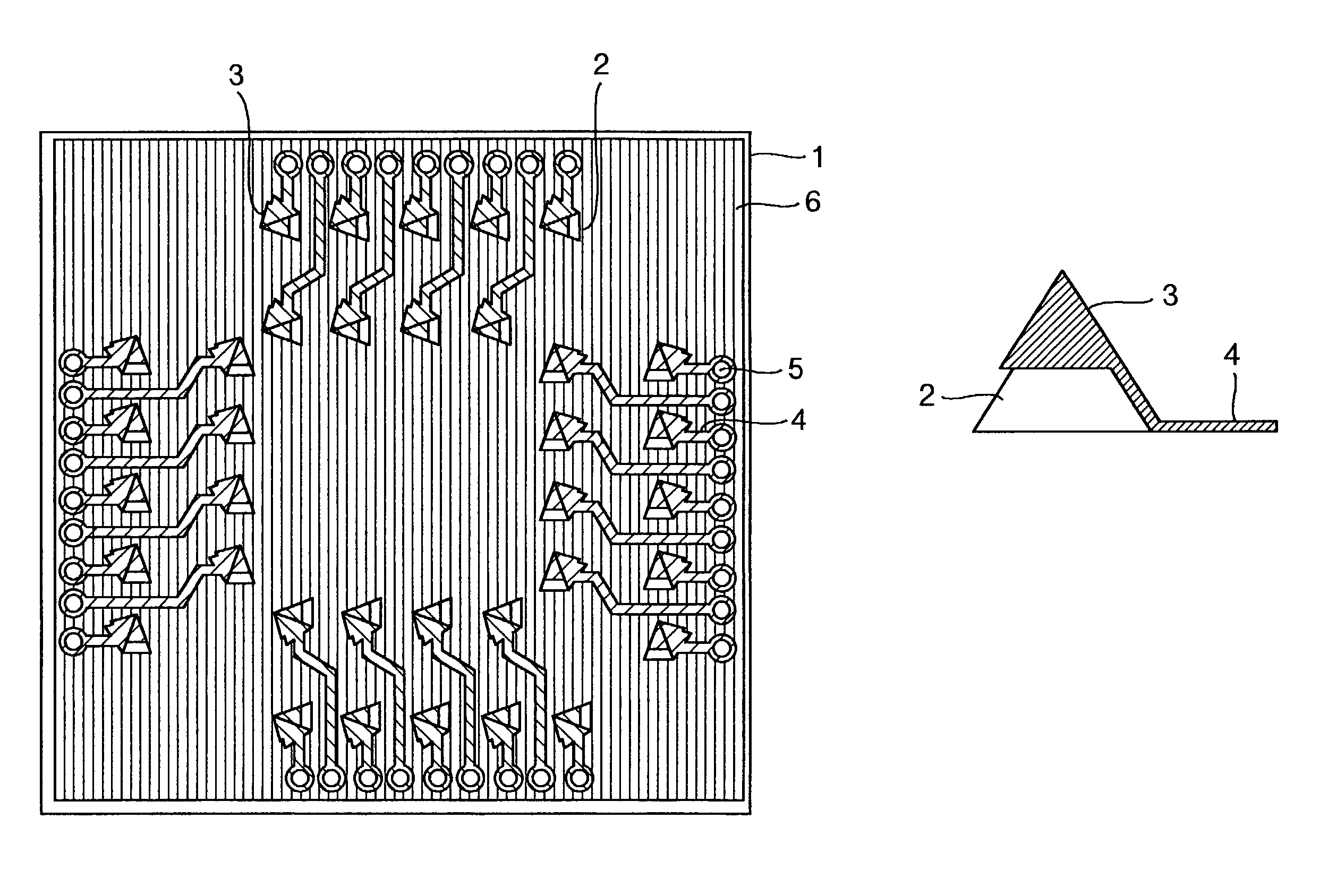
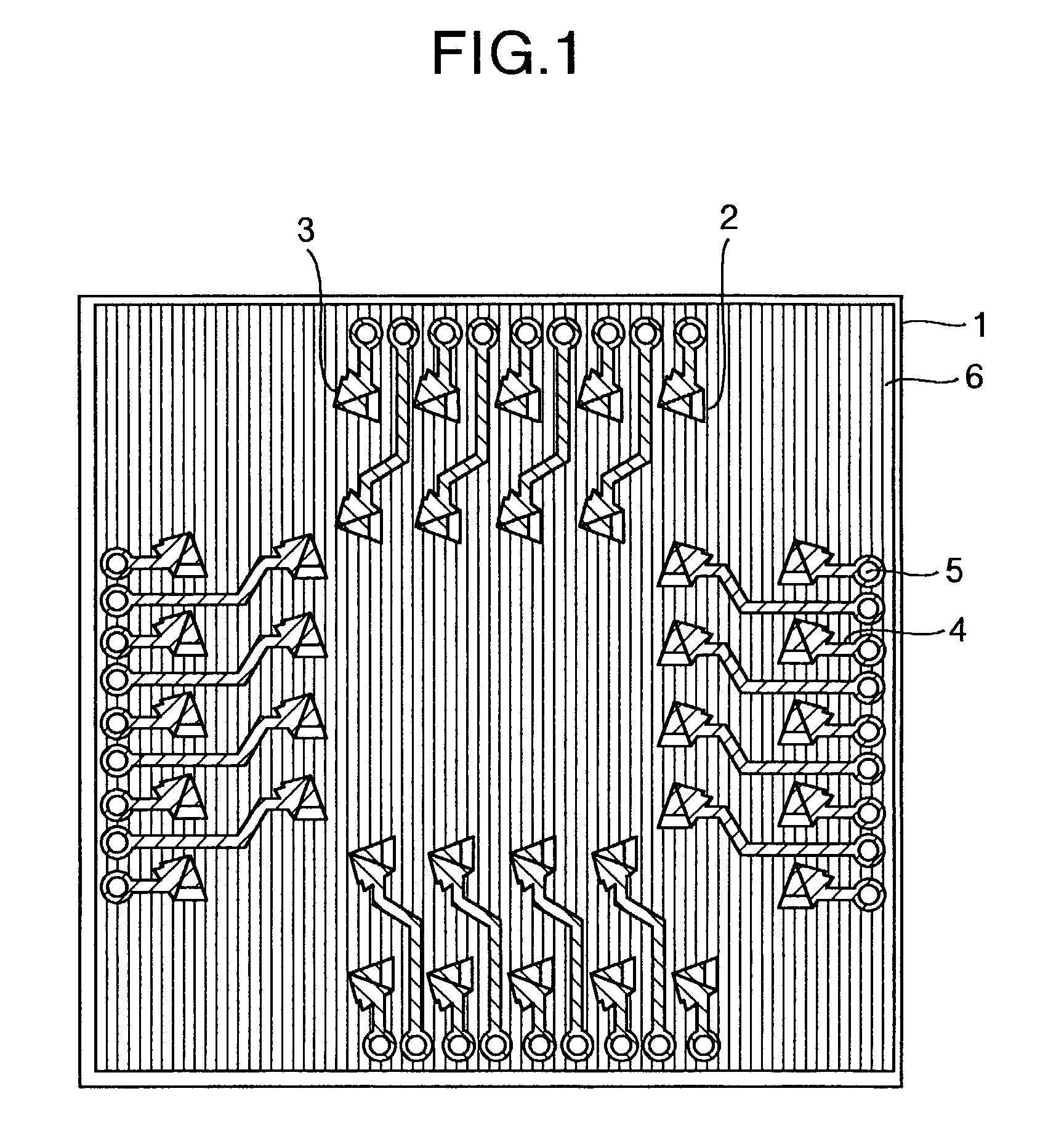
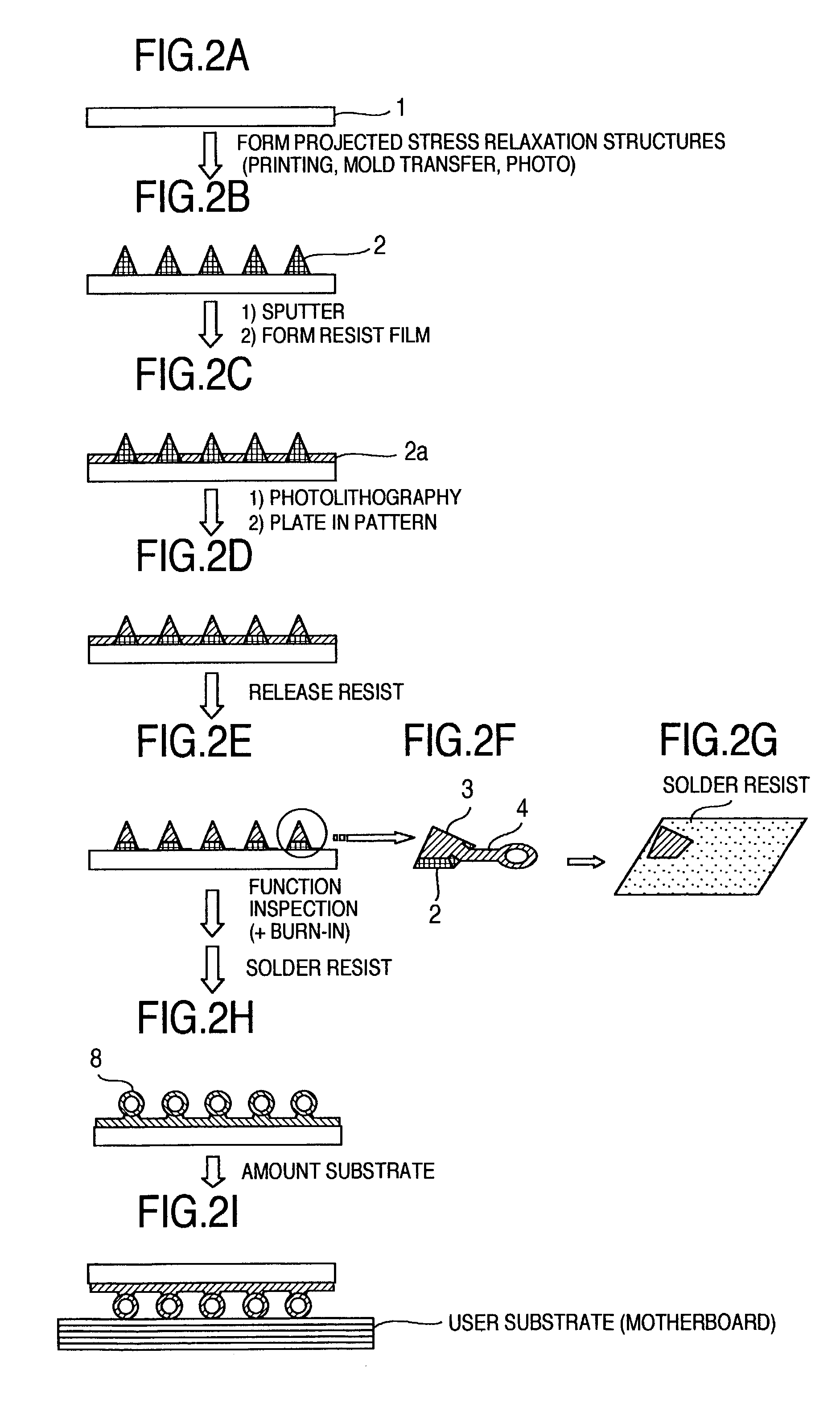
[0067]The present invention will be explained in connection with embodiments of the invention with reference to accompanying drawings. In all the drawings, parts having the same reference numerals or symbols indicate identical parts, and some of the parts are omitted to avoid double explanation in some cases. Further, for the sake of easy explanation, dimensional ratios between the parts are changed in the drawings.

[0068]In the embodiments, a semiconductor chip refers to a chip which is cut out from a semiconductor wafer having element circuits formed thereon and contains no wiring and stress relaxation structure. A semiconductor element refers to an element (in a semiconductor wafer state) which is before a semiconductor chip cut out from a semiconductor wafer having element circuit formed therein. That is, a difference between the semiconductor chip and semiconductor element depends on whether or not the semiconductor wafer is diced into individual chips. Further, a semiconductor ...


PUM


Abstract

A semiconductor device which includes a semiconductor chip, an insulating film formed on the semiconductor chip, a plurality of projected stress relaxation materials formed on the insulating film, projected electrodes covering at least tops of the stress relaxation materials, and wiring lines for electrically connecting the projected electrodes and element electrodes of the semiconductor chip.

Description

BACKGROUND OF THE INVENTION[0001]The present invention relates to semiconductor devices and structures for mounting the semiconductor devices and more particular, to a semiconductor device having a stress relaxation structure and a method for manufacturing the semiconductor device.[0002]In order to secure the reliability of connection between a semiconductor device and a substrate for mounting the semiconductor device thereon, a layer for relaxing a stress induced between the semiconductor device and substrate is formed therebetween.[0003]For example, JP-A-11-54649 (referred to as the first known example, hereinafter) discloses a semiconductor device wherein a layer having a low elastic modulus is formed on a semiconductor substrate and a plurality of metallic balls are formed on the low elastic modulus layer as external connection terminals.[0004]Also disclosed in JP-A-2-272737 (referred to as the second known example, hereinafter) is a projected electrode structure of semiconducto...

Claims


Application Information

Patent Timeline
Patent Type & Authority Patents(United States)
IPC IPC(8): H01L23/48H01L23/52H01L29/40H01L21/66H01L21/56H01L21/60H01L23/12H01L23/485
CPCH01L24/13H01L24/11H01L2221/68345H01L2224/114H01L2924/014H01L2224/116H01L2224/13099H01L2924/01004H01L2924/01011H01L2924/01013H01L2924/01015H01L2924/01029H01L2924/0103H01L2924/01075H01L2924/01078H01L2924/01079H01L2924/01082H01L2924/01092H01L2924/30105H01L2924/3025H01L2924/01005H01L2924/01006H01L2924/01033H01L2924/01047H01L2924/01084H01L2924/00H01L2924/351H01L2924/181H01L2924/12042H01L2224/11H01L2224/13H01L2224/05571H01L2224/05573H01L2224/023H01L2924/0001
Inventor YAMAGUCHI, YOSHIHIDETSUNODA, SHIGEHARUTENMEI, HIROYUKIHOZOJI, HIROSHIKANDA, NAOYA
Owner RENESAS TECH CORP
Why Eureka
Try Eureka