Integrated circuits with reduced interconnect overhead

a technology of integrated circuits and interconnect resources, applied in the field of integrated circuits, can solve the problems of consuming a large portion of the interconnect resources of the integrated circuit, unable to support other signal routing tasks, and inefficient use of general-purpose programmable logic resources to implement complex memory or digital signal processing circuits, etc., to achieve the maximum possible performance level

Inactive Publication Date: 2006-08-01
ALTERA CORP
View PDF18 Cites 26 Cited by
  • Summary
  • Abstract
  • Description
  • Claims
  • Application Information

AI Technical Summary

Benefits of technology

[0007]In accordance with the present invention, integrated circuits are provided that contain data compression and decompression circuitry. The compression and decompression circuitry can be used to minimize the amount of interconnect resources that are used to convey signals across the integrated circuits.
[0009]Parallel data signals from the region of programmable logic can be compressed by the programmable logic parallel-to-serial converter using time-division multiplexing. This reduces the number of parallel interconnect lines needed to carry the data. After the compressed data has been conveyed to its destination at the dedicated hardwired circuit, a dedicated hardwired serial-to-parallel converter can use time-division demultiplexing techniques to decompress the compressed data. The uncompressed version of the data may be provided to the dedicated hardwired circuit.
[0010]Data compression and decompression can also be used to minimize consumption of interconnect resources that are used to convey data from the dedicated hardwired circuit to other logic. For example, a dedicated hardwired parallel-to-serial converter circuit can use time-division multiplexing to compress data signals (e.g., data signals that have been processed by digital signal processing circuitry in the dedicated hardwired circuit). These compressed data signals can be conveyed across an integrated circuit using a reduced number of parallel interconnect lines. A programmable logic serial-to-parallel converter that is formed from user-configured programmable logic can use time-division demultiplexing techniques to decompress the data that was compressed using the hardwired parallel-to-serial converter.
[0017]In the third mode of operation, the switching circuitry and programmable logic are configured so that interconnection resources are allocated to serving the second dedicated hardwired circuit. The programmable logic for the programmable logic parallel-to-serial converter need not be used to form the programmable logic parallel-to-serial converter and can therefore be used for other programmable logic functions. All of the interconnect resources associated with the first and second dedicated hardwired circuit are available to serve the second dedicated hardwired circuit, so the second dedicated hardwired circuit can operate at its maximum possible performance level.

Problems solved by technology

However, using general-purpose programmable resources to implement complex memory or digital signal processing circuits can be inefficient.
As an example, implementing an 18-bit×18-bit multiplier using general-purpose programmable logic resources may consume ten times more circuit real estate than implementing the same type of multiplier using a dedicated multiplier circuit.
When large groups of interconnect lines such as the interconnect lines traditionally associated with memory and signal processing circuit blocks extend across a significant portion of an integrated circuit, a correspondingly large portion of the interconnect resources of the integrated circuit are consumed and are therefore not available to support other signal routing tasks.

Method used


Image

  • Integrated circuits with reduced interconnect overhead
  • Integrated circuits with reduced interconnect overhead
  • Integrated circuits with reduced interconnect overhead

Examples


Embodiment Construction

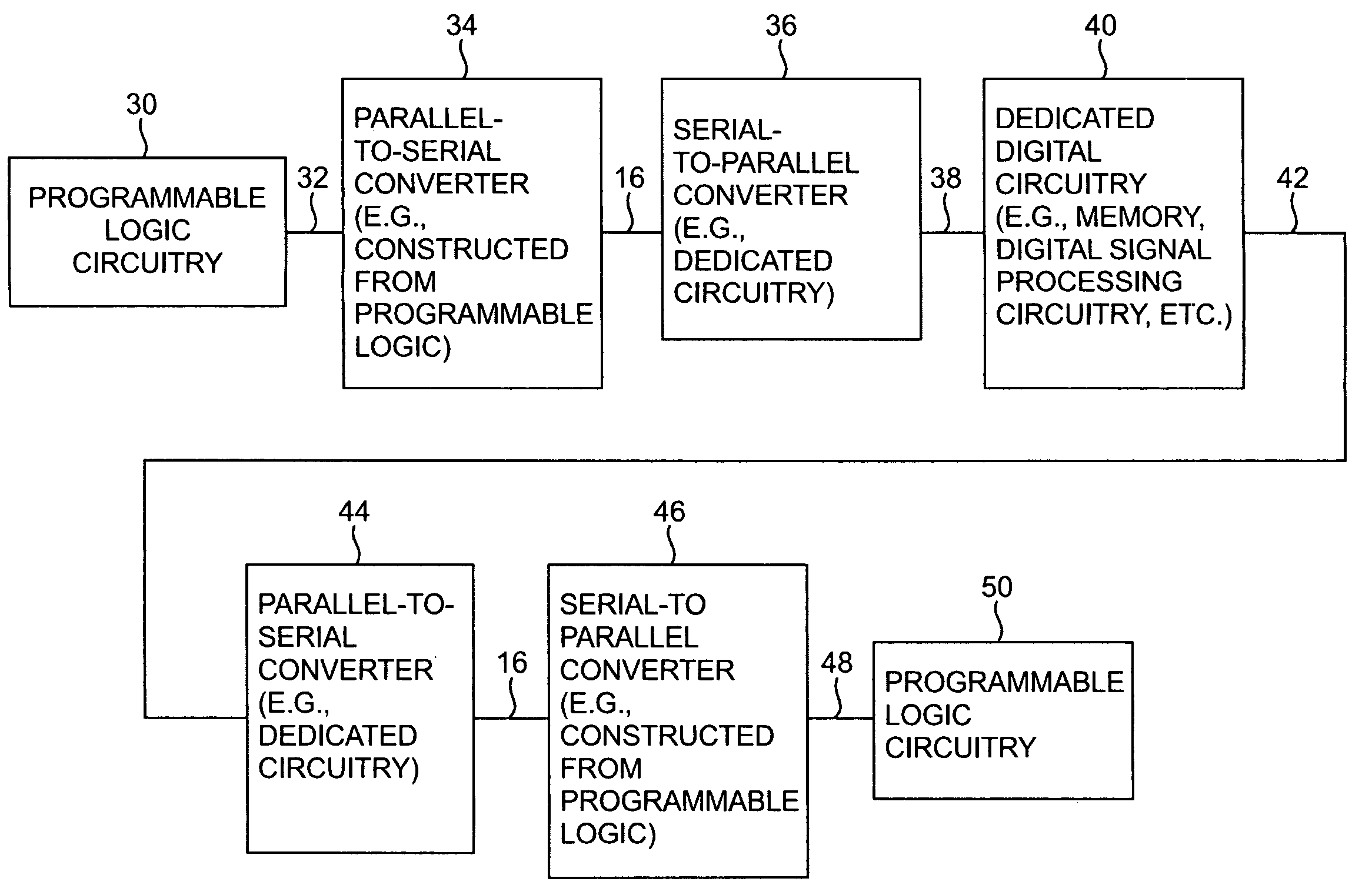
[0025]The present invention relates to circuit arrangements that may be used to minimize the consumption of interconnect resources on an integrated circuit and thereby lower circuit cost while maintaining desired levels of performance. The invention applies to any suitable integrated circuits. For clarity, the present invention will sometimes be described in the context of programmable logic device integrated circuits. This is, however, merely illustrative.

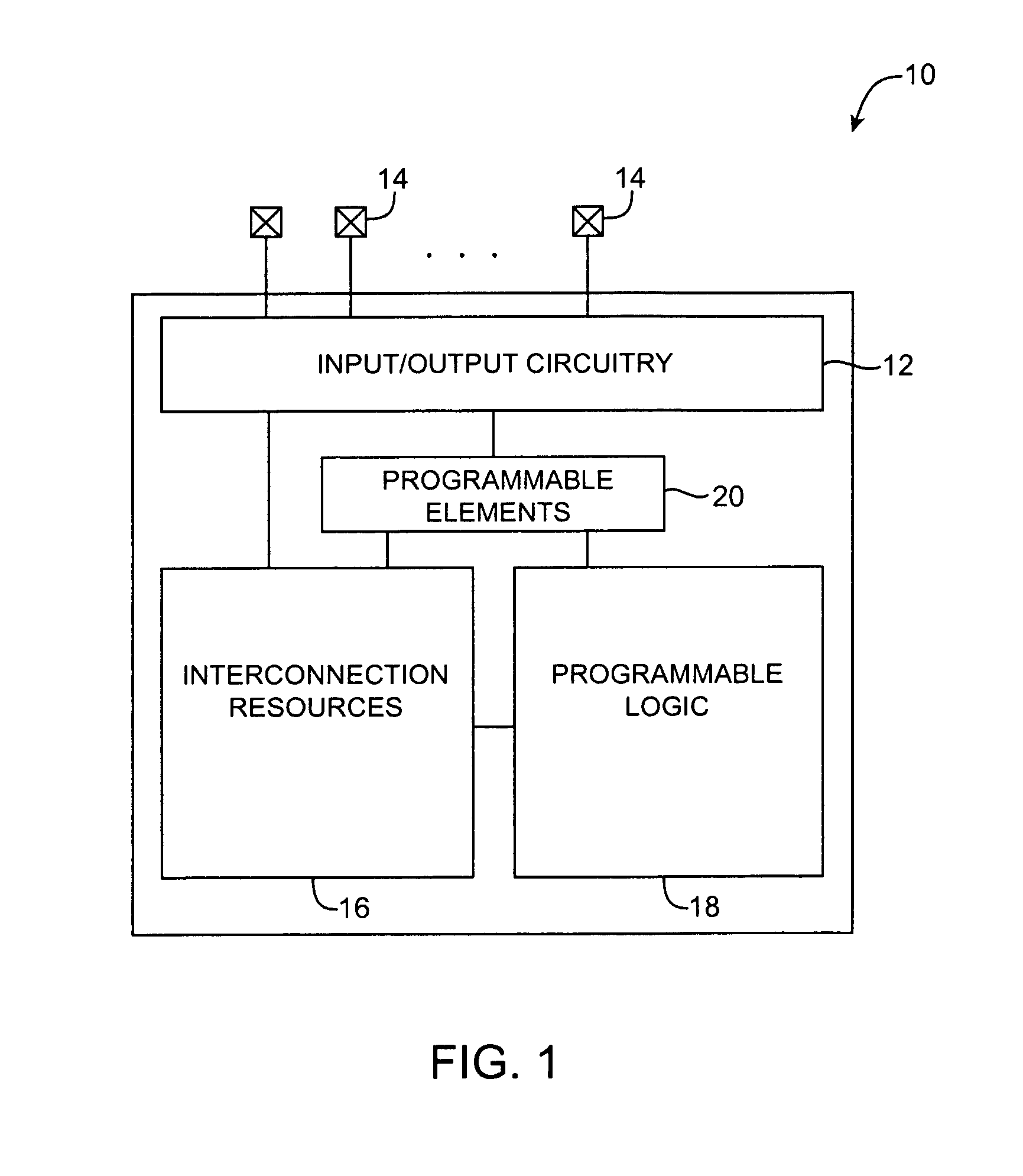
[0026]An illustrative programmable logic device 10 in accordance with the present invention is shown in FIG. 1.

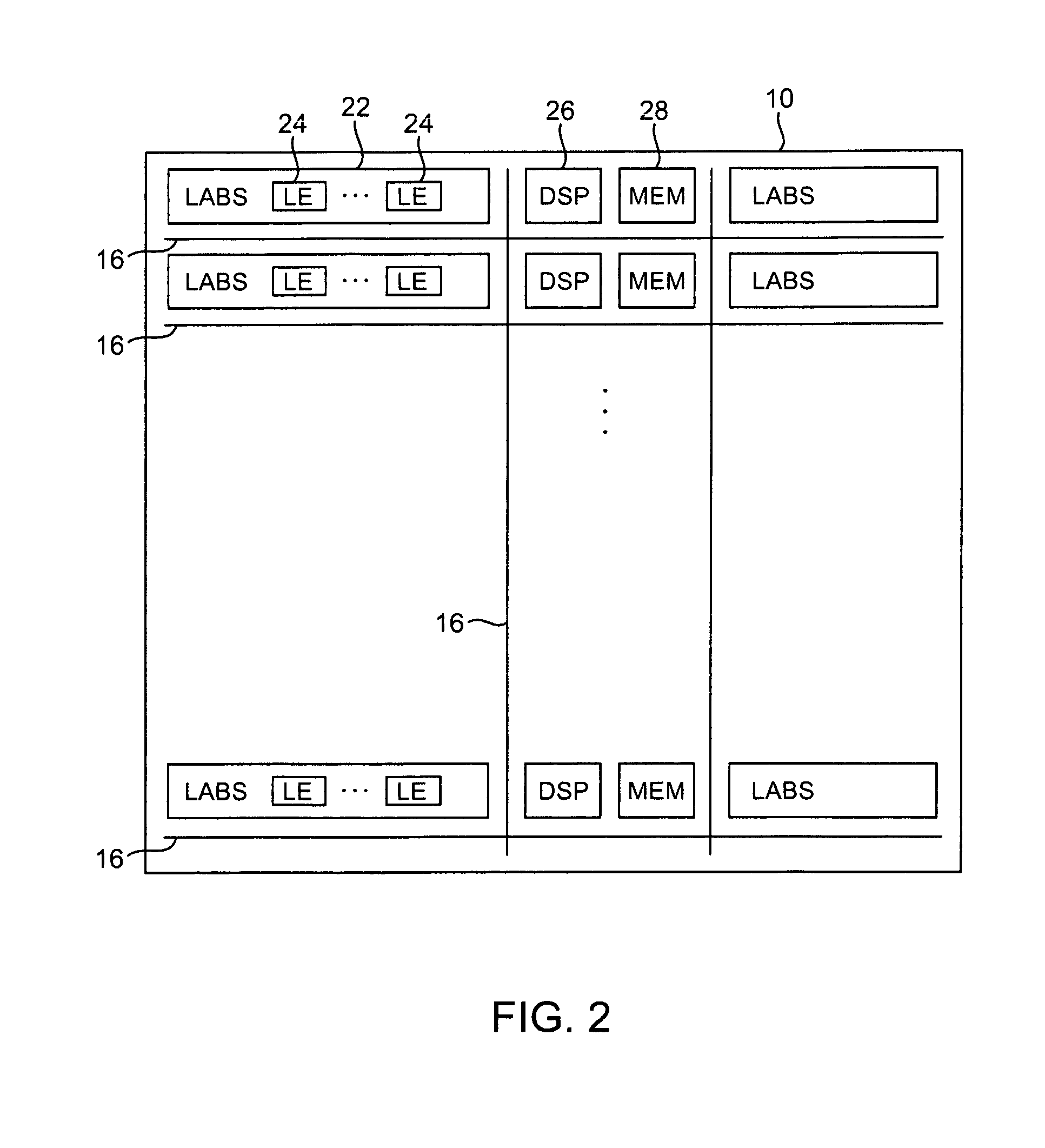
[0027]Programmable logic device 10 may have input / output circuitry 12 for driving signals off of device 10 and for receiving signals from other devices via input / output pins 14. Interconnection resources 16 such as vertical and horizontal conductive lines may be used to route signals on device 10. Programmable logic 18 may include combinational and sequential logic circuitry. The programmable logic 18 may be configured to...


PUM


Abstract

Integrated circuits are provided that use on-chip data compression and decompression to minimize consumption of interconnect resources. Parallel-to-serial converter circuitry can use time-division multiplexing techniques to compress data. The compressed data may be conveyed between circuit blocks on the integrated circuit using a reduced number of parallel interconnect conductors. After the compressed data has been conveyed to its destination, a serial-to-parallel converter may use time-division demultiplexing techniques to decompress the data. Interconnect resources may be shared by dedicated circuits. With this arrangement, signals can be selectively steered through the appropriate dedicated circuitry to either maximize performance or to use compression and decompression to minimize interconnect resource consumption.

Description

BACKGROUND OF THE INVENTION[0001]This invention relates to integrated circuits such as programmable logic device integrated circuits, and more particularly, to circuitry that compresses parallel data into a more serialized format to reduce the overhead associated with providing large numbers of parallel interconnect lines when conveying data across a chip.[0002]Integrated circuits such as programmable logic devices typically contain logic resources whose operation can be programmed using configuration data. A user can customize a programmable logic device to perform a desired logic function by loading appropriate configuration data into the device. The programmable resources on a programmable logic device can be used to implement memory and digital signal processing functions. However, using general-purpose programmable resources to implement complex memory or digital signal processing circuits can be inefficient. As an example, implementing an 18-bit×18-bit multiplier using general...

Claims


Application Information

Patent Timeline
Patent Type & Authority Patents(United States)
IPC IPC(8): G06F7/38H03K19/173H04Q7/00H04Q7/28
CPCH03K19/17732H03K19/17784H03K19/17736
Inventor LEE, KWAN YEELANGHAMMER, MARTINBURNEY, ALI H.
Owner ALTERA CORP
Why Eureka
Try Eureka