
Low-power memory write circuits

a write circuit and memory technology, applied in the field of low-power memory write circuits, can solve the problems of limiting the applicability of the memory to the electronic device, increasing the size and complexity increasing the power consumption of the integrated circuit, so as to reduce the overall power consumption of the memory

Active Publication Date: 2006-08-01
ORACLE INT CORP
View PDF3 Cites 4 Cited by
  • Summary
  • Abstract
  • Description
  • Claims
  • Application Information

AI Technical Summary

Benefits of technology

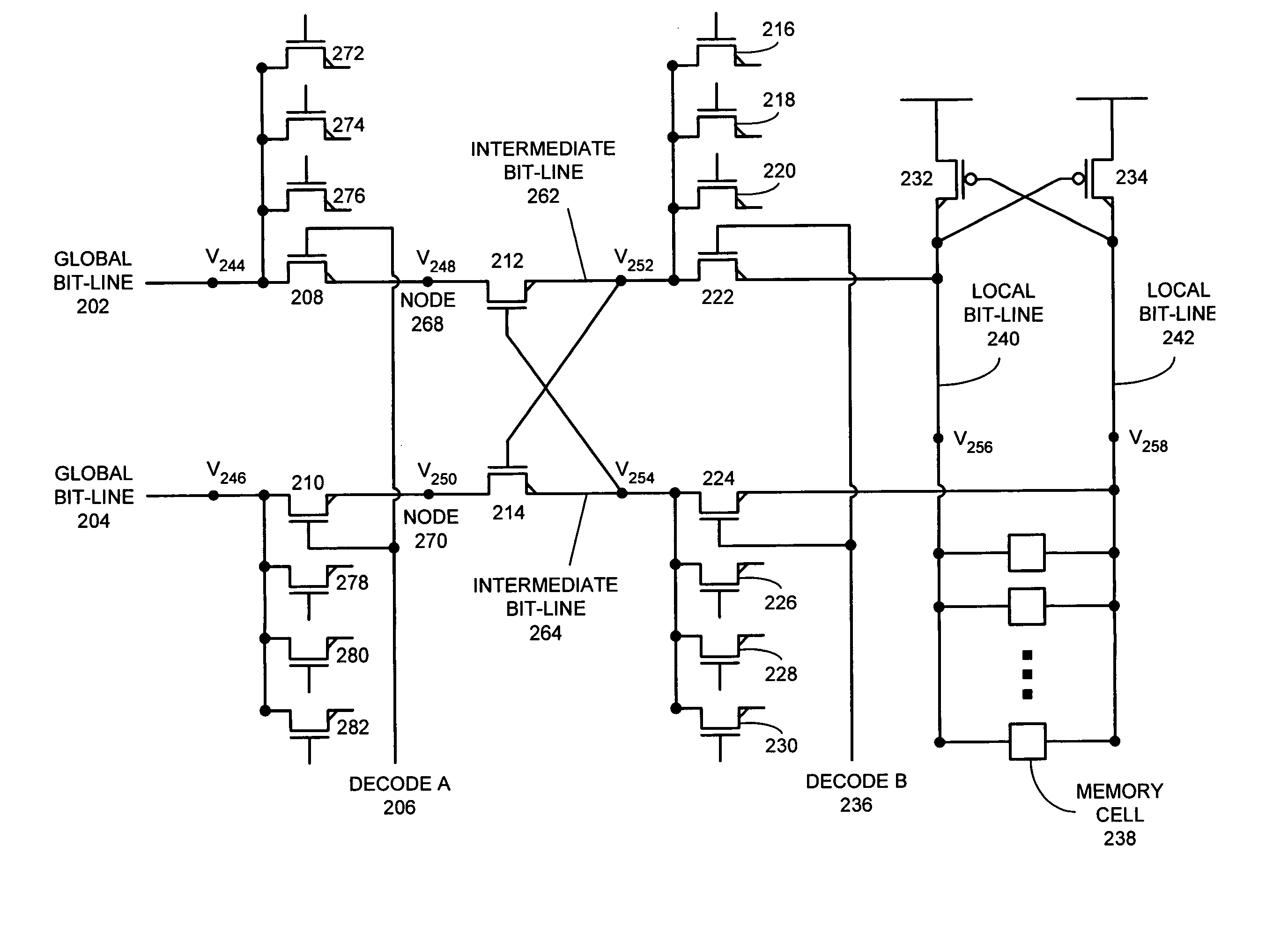
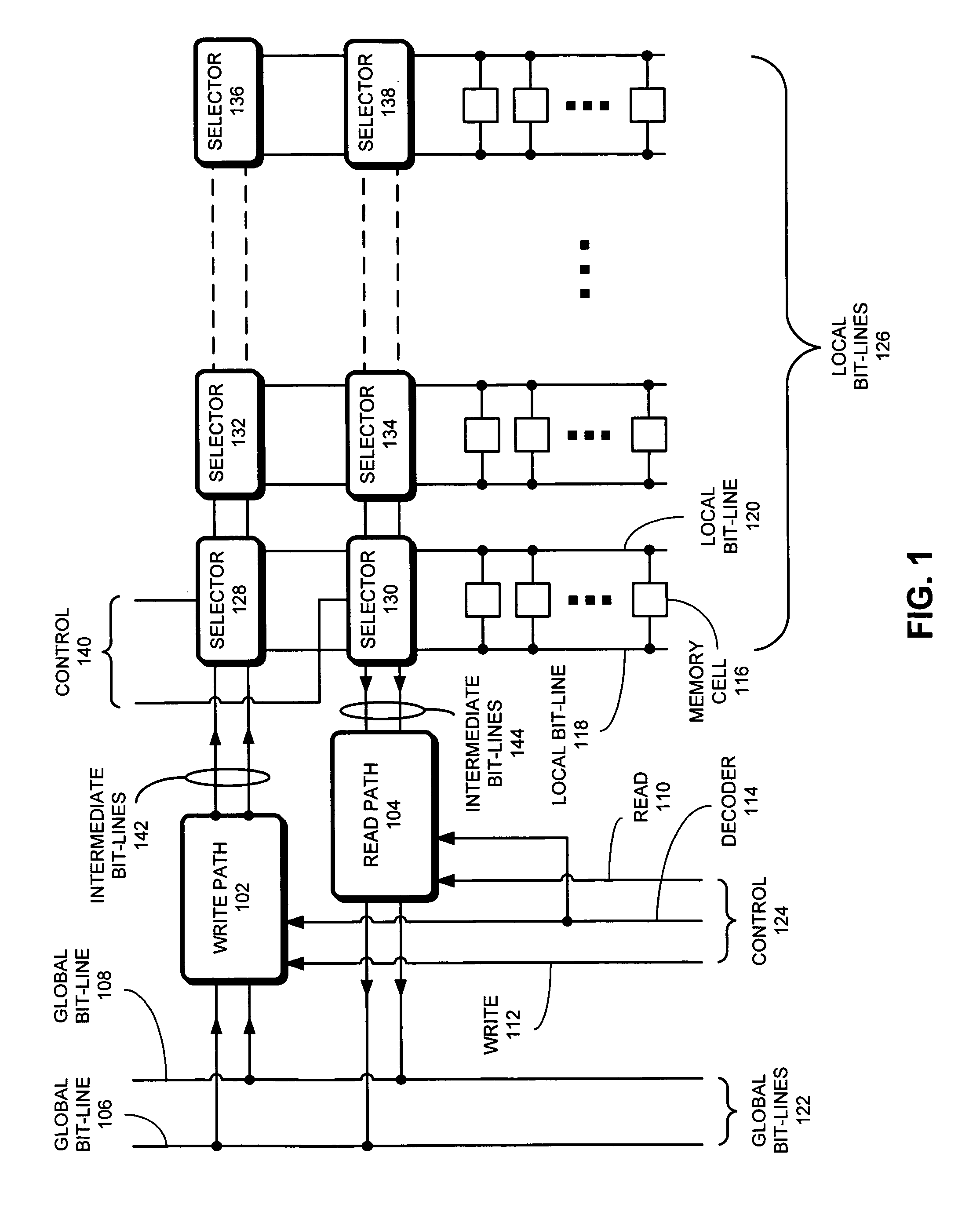
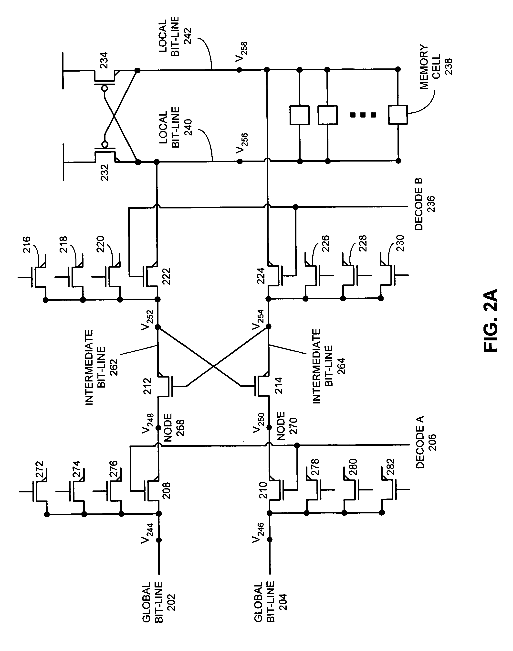
[0013]One embodiment of the present invention provides a system that writes to a cell in a memory using a low-voltage-swing signal across a pair of global bit-lines. During operation, the system receives a low-voltage-swing signal across a pair of global bit-lines. Note that the voltage swing of the low-voltage-swing signal may be less than the voltage swing required for stable (reliable) writes to a memory cell. Next, the system converts the low-voltage-swing signal to a high-voltage-swing signal. Note that the voltage swing of the high-voltage-swing signal can be greater than or equal to the voltage swing required for stable (reliable) writes to the memory cell. The system then writes to the memory cell by applying the high-voltage-swing signal across a pair of local bit-lines that are coupled with the memory cell. Note that by using low-voltage-swing signals instead of high-voltage-swing signals on the long and high-capacitance global bit-lines, the present invention reduces the overall power consumption of the memory.
[0016]In a further variation on this embodiment, the direct or indirect coupling of the sources of the first pair of cross-coupled NMOS transistors is facilitated using a pair of selection transistors having a common gate voltage.
[0017]In a further variation on this embodiment, the system converts the low-voltage-swing signal to the high-voltage-swing signal using a second pair of cross-coupled NMOS transistors to quickly discharge a local bit-line in the pair of local bit-lines, thereby quickly creating the high-voltage-swing signal across the pair of local bit-lines.

Problems solved by technology

These advances can be largely attributed to the exponential increase in the size and complexity of integrated circuits.
Unfortunately, in conjunction with the increase in size and complexity, the power consumption of integrated circuits has also increased.
In many scenarios, the power consumption of a memory can limit its applicability to the electronic device.
For example, a memory's power consumption can become a limiting factor due to the system's inadequate heat dissipation capabilities.
Similarly, due to the scarcity of battery power in a mobile device, a memory's power consumption can become a limiting factor.
As a result, during writes, global bit-lines can end up using a significant fraction of the memory's power consumption.

Method used


Image

  • Low-power memory write circuits
  • Low-power memory write circuits
  • Low-power memory write circuits

Examples


Embodiment Construction

[0023]The following description is presented to enable any person skilled in the art to make and use the invention, and is provided in the context of a particular application and its requirements. Various modifications to the disclosed embodiments will be readily apparent to those skilled in the art, and the general principles defined herein may be applied to other embodiments and applications without departing from the spirit and scope of the present invention. Thus, the present invention is not limited to the embodiments shown, but is to be accorded the widest scope consistent with the principles and features disclosed herein.

Structure of a Memory Chip

[0024]Memory chips in a VLSI process are typically organized hierarchically, with individual memory cells grouped together to share data lines. These data lines are called “local bit-lines,” and are paired as true and complement wires. The memory cells that are coupled with these local bit-lines are then grouped together to form larg...


PUM


Abstract

One embodiment of the present invention provides a system that writes to a cell in a memory using a low-voltage-swing signal across a pair of global bit-lines. During operation, the system receives a low-voltage-swing signal across a pair of global bit-lines, which is too low to reliably write the memory cell. Next, the system converts the low-voltage-swing signal to a high-voltage-swing signal, which is adequate to reliably write the memory cell. The system then writes to the memory cell by applying the high-voltage-swing signal across a pair of local bit-lines that are coupled to the memory cell. The use of low-voltage-swing signals on the global bit-lines reduces overall power consumption. Furthermore, in one embodiment of the present invention, the voltage conversion is achieved using a pair of cross-coupled NMOS transistors whose sources are directly or indirectly coupled with the global bit-lines, and whose drains are directly or indirectly coupled with the local bit-lines.

Description

BACKGROUND[0001]1. Field of the Invention[0002]This invention relates to the process of writing to memory. More specifically, this invention relates to the process of writing data into memory using low-voltage-swing signals on global bit-lines.[0003]2. Related Art[0004]Rapid advances in computing technology have made it possible to perform trillions of computational operations each second on data sets that are sometimes as large as a trillion bytes. These advances can be largely attributed to the exponential increase in the size and complexity of integrated circuits.[0005]Unfortunately, in conjunction with the increase in size and complexity, the power consumption of integrated circuits has also increased. As a result, there is a strong need for integrated circuits that consume less power without sacrificing functionality.[0006]Almost every electronic device contains some form of memory. In many scenarios, the power consumption of a memory can limit its applicability to the electron...

Claims


Application Information

Patent Timeline
IPC IPC(8): G11C7/00
CPCG11C7/1048G11C7/1096G11C7/1078G11C2207/2227
Inventor PROEBSTING, ROBERT J.HO, RONALDDROST, ROBERT J.
Owner ORACLE INT CORP
Learn More