Signal processing semiconductor integrated circuit device and wireless communication system

a technology of integrated circuits and semiconductors, applied in the direction of transmission, frequency demodulator arrangements, substation equipment, etc., can solve the problems of extremely small circuit scale and large circuit scale, and achieve the effects of reducing the number of parts in the communication system, increasing the packing density, and reducing the siz

Inactive Publication Date: 2006-08-01
RENESAS ELECTRONICS CORP
View PDF12 Cites 24 Cited by
  • Summary
  • Abstract
  • Description
  • Claims
  • Application Information

AI Technical Summary

Benefits of technology

[0018]Further, a reception-system circuit having the above-described configuration, a transmission-system circuit including a modulation circuit which modulates a transmit signal, and frequency converting means which combines the modulated signal with an oscillation signal to thereby effect frequency conversion on the combined signal, a control-system circuit which controls the reception-system circuit and the transmission-system circuit, and an oscillation-system circuit which generates an oscillation signal or an oscillation control signal combined by the reception-system circuit and the transmission-system circuit, are formed on a single semiconductor substrate so as to constitute a signal processing semiconductor integrated circuit device. Thus, it is possible to implement a one-chip transmitting/receiving LSI, reduce the number of parts in a communication system, increase packing density and hence bring a cellular phone into less size.
[0019]There is provided a wireless communication system comprising a signal processing semiconductor integrated circuit device of the above one chip; and a baseband circuit brought into a semiconductor integrated circuit, which performs signal processing for performing the conversion of a signal outputted from the reception-system circuit to a voice signal and the conversion of the voice signal to the transmit signal, and controls the signal processing semiconductor integrated circuit device, wherein a command signal for activating the voltage reference circuit and a command signal for activating the frequency converting means and the second amplifier circuit are supplied from the baseband circuit to the signal processing semiconductor integrated circuit device. Thus, there is no need to provide a control LSI like a microprocessor, which controls the entire system separately from the baseband circuit. It is also possible to reduce the number of parts in the communication system, increase packing density and hence bring a cellular telephone into less size.
[0020]The command signal for activating the voltage reference circuit and the command signal for activating the frequency converting means and the second amplifier circuit may preferably be supplied from the baseband circuit to the control-system circuit lying within the signal processing semiconductor integrated circuit device. Thus, the baseband circuit may simply supply a command to the control-system circuit of the signal processing semiconductor integrated circuit device, a

Problems solved by technology

The superheterodyne system is accompanied by a problem that since the process of demodulating the received signal is done after the received signal is temporarily down-converted to the intermediate frequency signal, a circuit scale becomes large.
However, the present inventors have found out defects or defective conditions in that in the direct conversion

Method used


Image

  • Signal processing semiconductor integrated circuit device and wireless communication system
  • Signal processing semiconductor integrated circuit device and wireless communication system
  • Signal processing semiconductor integrated circuit device and wireless communication system

Examples


Embodiment Construction

[0035]Preferred embodiments of the present invention will hereinafter be described with reference to the accompanying drawings.

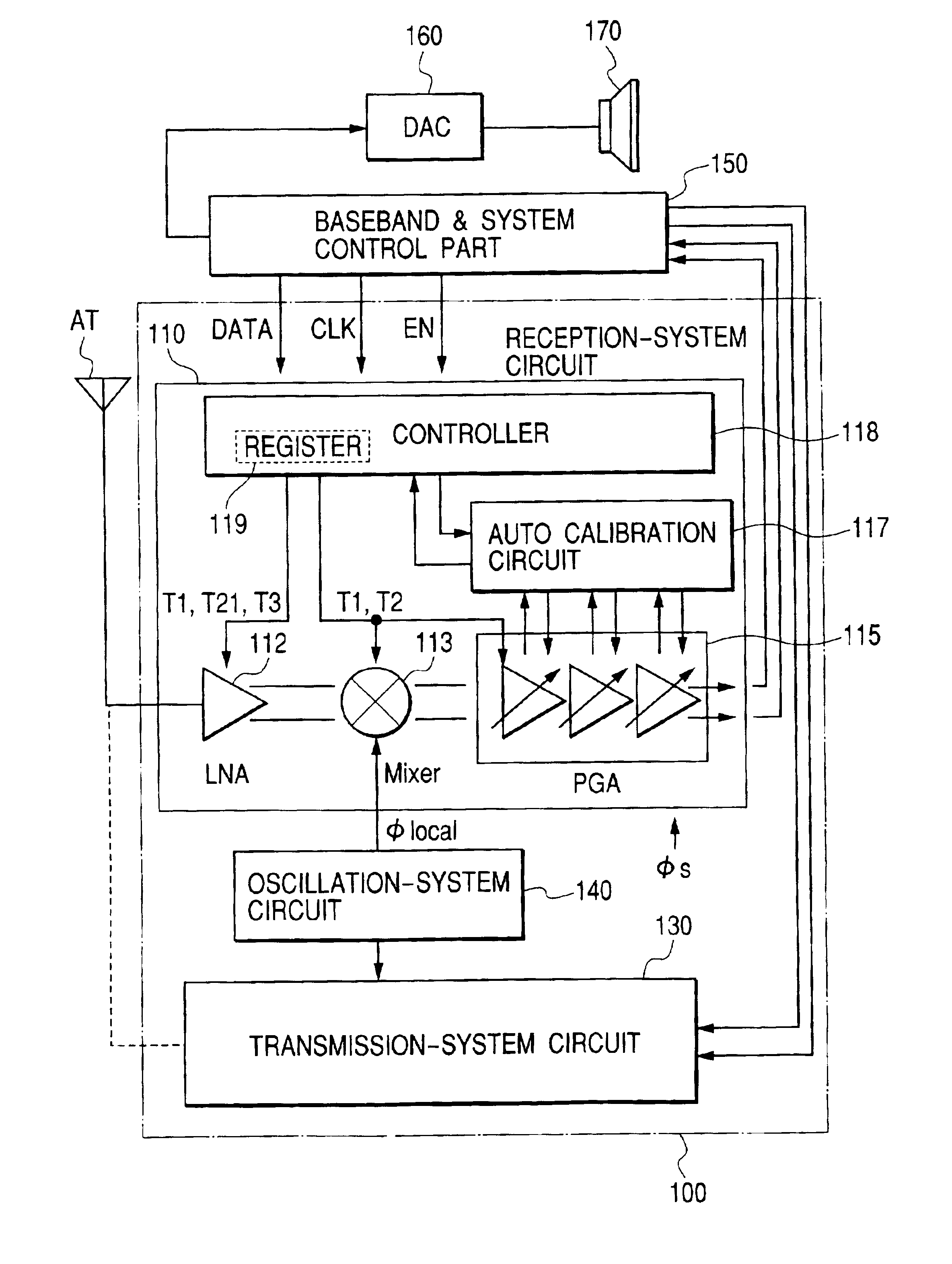
[0036]FIG. 1 shows a configurational example of a signal processing system for a cellular telephone, which is suitable for application of the present invention thereto.

[0037]In FIG. 1, AT indicates an antenna which transmits a signal wave therefrom and receives it therein. Reference numeral 110 indicates a direct conversion reception-system circuit which demodulates and amplifies the signal received by the antenna AT without intervention of an intermediate frequency and converts it to a baseband signal, reference numeral 130 indicates a transmission-system circuit which modulates and frequency-converts the baseband signal to be transmitted via the antenna AT, reference numeral 140 indicates an oscillation-system circuit which generates a local oscillation signal φlocal necessary for the frequency conversion at each of the reception-system circuit 110 and the...


PUM


Abstract

Disclosed herein is a direct conversion type signal processing semiconductor integrated circuit device capable of suppressing a DC voltage variation in the output of a variable gain amplifier upon the transition to a reception mode, reproducing stable receiving characteristics and improving receiving sensitivity. In the signal processing semiconductor integrated circuit device, voltage reference circuits for generating reference voltages for controlling or restricting currents for current sources for supplying operating currents for amplifiers constituting a reception-system circuit are boosted upon the transition from an idle mode or the like to the reception mode to allow the currents to flow into the constant-current sources of the amplifiers after the stabilization of the generated reference voltages.

Description

BACKGROUND OF THE INVENTION[0001]The present invention relates to a semiconductor integrated circuit technology and a technology effective for application to a reduction in DC offset of each of multistage-connected amplifiers, e.g., a technology effective for application to a direct conversion type signal processing LSI (Large Scale Integration) for processing transmit and receive signals used in a cellular telephone.[0002]A system called a “superheterodyne system” has heretofore been known for a radio communication LSI for processing transmit and receive signals used in a cellular phone. Such a configuration as shown in FIG. 10 by way of example is considered as a reception-system circuit based on the superheterodyne system. Namely, as illustrated in FIG. 10, the reception-system circuit comprises a bandwidth limiting filter (FLT) 111 comprising a SAW filter which eliminates an unnecessary wave from a signal received by an antenna AT, a low noise amplifier (LNA) 112 which amplifies...

Claims


Application Information

Patent Timeline
IPC IPC(8): H04B1/04H03F1/00H03D3/00H03D7/14H04B1/16H04B1/30
CPCH03D3/002H03D7/1433H04B1/30H03D7/1458H03D2200/009H03D2200/0033H03D2200/0043H03D2200/0047H03D2200/0025
Inventor OONO, IKUYAMATSUI, TOSHIKIOOSAWA, HIROTAKA
Owner RENESAS ELECTRONICS CORP
Why Eureka
Try Eureka