Multiple clock domain microprocessor

a microprocessor and clock domain technology, applied in the field of microprocessors, can solve the problems that benchmarks have not traditionally been candidates for voltage and frequency scaling

Active Publication Date: 2006-08-08
UNIVERSITY OF ROCHESTER
View PDF8 Cites 30 Cited by
  • Summary
  • Abstract
  • Description
  • Claims
  • Application Information

AI Technical Summary

Benefits of technology

[0040]To achieve the above and other objects, the present invention is directed to a multiple clock domain (MCD) microarchitecture, which uses a globally-asynchronous, locally-synchronous (GALS) clocking style. In an MCD microprocessor each functional block operates with a separately generated clock, and synchronizing circuits ensure reliable inter-domain communication. Thus, fully synchronous design practices are used in the design of each domain. Although the inter-domain synchronization increases the number of clock cycles required to run a given application, an MCD microprocessor affords a number of potential advantages over a singly clocked design:
[0042]The independence of each local domain clock implies no global clock skew requirement, permitting potentially higher frequencies within each domain and greater scalability in future process generations.
[0044]Using separate voltage inputs, external voltage regulators, and controllable clock frequency circuits in each clock domain allows for finer grained dynamic voltage and frequency scaling, and thus lower energy, than can be achieved with single clock, single-core-voltage systems.
[0047]We disclose a multiple clock domain (MCD) microarchitecture, which uses a globally-asynchronous, locally-synchronous (GALS) clocking style along with dynamic voltage and frequency scaling in order to maximize performance and energy efficiency for a given application. Our design uses existing queue structures in a superscalar processor core to isolate the different clock domains in a way that minimizes the need for inter-domain synchronization.
[0049]Our current analysis uses an off-line algorithm to determine the points in the program at which different domains should change frequency and voltage. Variations within the scope of the invention include effective on-line algorithms, including approaches for effective scaling of the front end, as well as the ability to deliver tunable on-chip voltage and frequency with low latency.

Problems solved by technology

Unlike rate-based multimedia applications, these benchmarks have not traditionally been candidates for voltage and frequency scaling.

Method used


Image

  • Multiple clock domain microprocessor
  • Multiple clock domain microprocessor
  • Multiple clock domain microprocessor

Examples


Embodiment Construction

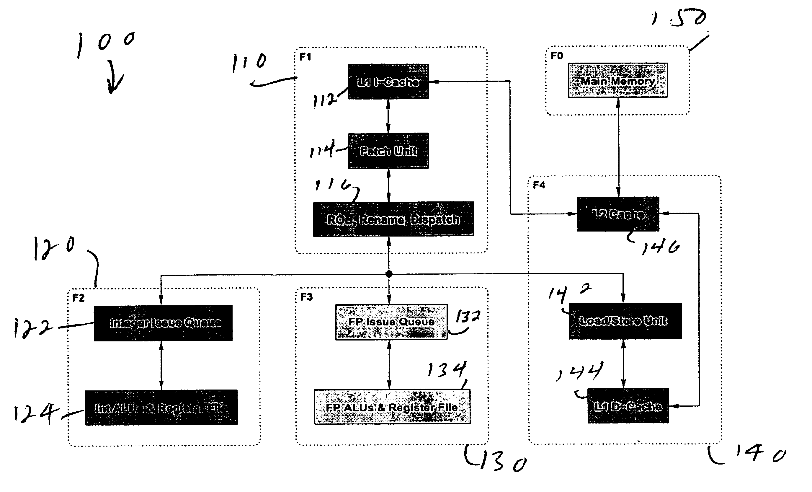
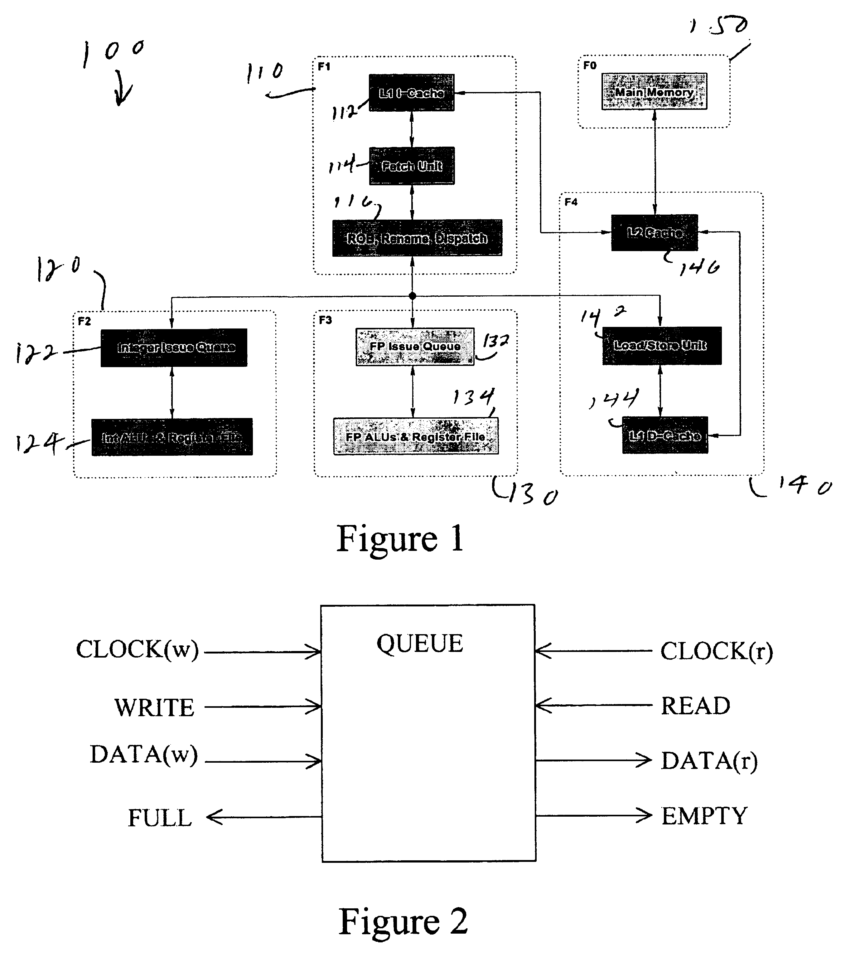
[0061]Matzke has estimated that as technology scales down to a 0.1 μm feature size, only 16% of the die will be reachable within a single clock cycle [24]. Assuming a chip multiprocessor with two processors per die, each processor would need to have a minimum of three equal-size clock domains. The preferred embodiment uses four domains, one of which includes the L2 cache, so that domains may vary somewhat in size and still be covered by a single clock. In effect, we treat the main memory interface as a fifth clock domain, external to the MCD processor, and always running at full speed.

[0062]In choosing the boundaries between domains, we attempted to identify points where (a) there already existed a queue structure that served to decouple different pipeline functions, or (b) there was relatively little inter-function communication. Our four chosen domains, shown in the architecture 100 of FIG. 1, comprise the front end 110 (including instruction cache 112, fetch unit 114, and branch ...


PUM


Abstract

A multiple clock domain (MCD) microarchitecture uses a globally-asynchronous, locally-synchronous (GALS) clocking style. In an MCD microprocessor each functional block operates with a separately generated clock, and synchronizing circuits ensure reliable inter-domain communication. Thus, fully synchronous design practices are used in the design of each domain.

Description

REFERENCE TO RELATED APPLICATION[0001]The present application claims the benefit of U.S. Provisional Patent Application No. 60 / 441,759, filed Jan. 23, 2003, whose disclosure is hereby incorporated by reference in its entirety into the present disclosure.STATEMENT OF GOVERNMENT INTEREST[0002]This work was supported in part by NSF grants CCR-9701915, CCR-9702466, CCR-9705594, CCR-9811929, EIA-9972881, CCR-9988361, and EIA-0080124; by DARPA / ITO under AFRL contract F29601-00-K-0182. The government has certain rights in the invention.FIELD OF THE INVENTION[0003]The present invention is directed to microprocessors and more particularly to microprocessors having multiple clock domains.DESCRIPTION OF RELATED ART[0004]The continuing push for higher microprocessor performance has led to unprecedented increases in clock frequencies in recent years. While the Pentium III microprocessor broke the 1 GHz barrier in 2000, the Pentium IV is currently shipping at 2 GHz. At the same time, due to issue...

Claims


Application Information

Patent Timeline
Patent Type & Authority Patents(United States)
IPC IPC(8): G06F1/04G06F1/10G06F1/32
CPCG06F1/10G06F1/3203G06F1/324G06F1/3296G06F1/3243Y02B60/1285Y02B60/1217Y02B60/1239Y02D10/00G06F1/04
Inventor ALBONESI, DAVIDSEMERARO, GREGMAGKLIS, GRIGORIOSSCOTT, MICHAEL L.BALASUBRAMONIAN, RAJEEVDWARKADAS, SANDHYA
Owner UNIVERSITY OF ROCHESTER
Why Eureka
Try Eureka