Method of forming a nanocluster charge storage device

a charge storage device and nanocrystal technology, applied in the field of semiconductor devices, can solve the problems of oxidizing nanocrystals and undesirable increasing the bottom dielectric thickness

Active Publication Date: 2006-08-15
TAIWAN SEMICON MFG CO LTD
View PDF8 Cites 30 Cited by
  • Summary
  • Abstract
  • Description
  • Claims
  • Application Information

AI Technical Summary

Problems solved by technology

This oxidizing ambient may penetrate the control dielectric of the charge storage transistors thereb

Method used


Image

  • Method of forming a nanocluster charge storage device
  • Method of forming a nanocluster charge storage device
  • Method of forming a nanocluster charge storage device

Examples


Embodiment Construction

)

[0011]The following discussion is intended to provide a detailed description of at least one example of the invention and should not be taken to be limiting of the invention itself. Rather, any number of variations may fall within the scope of the invention which is properly defined in the claims following this description.

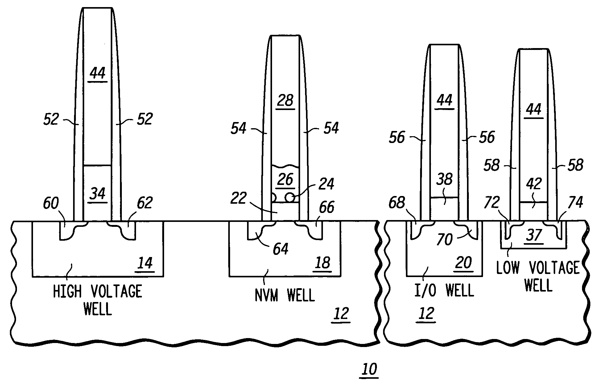
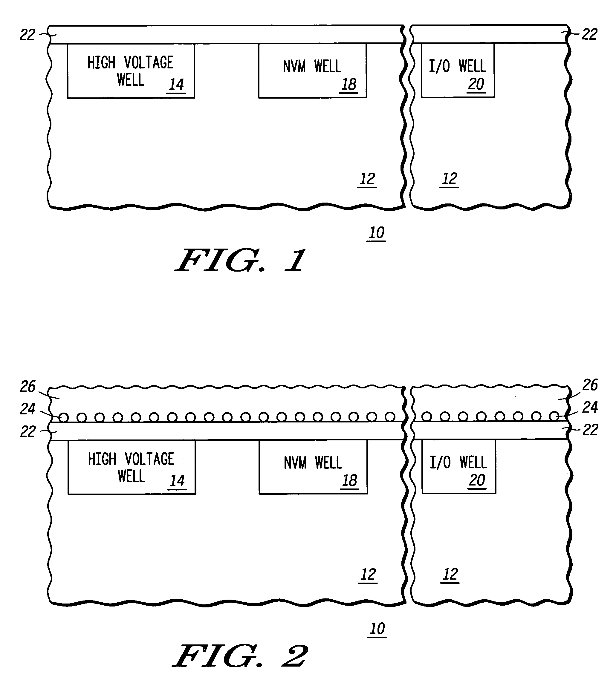
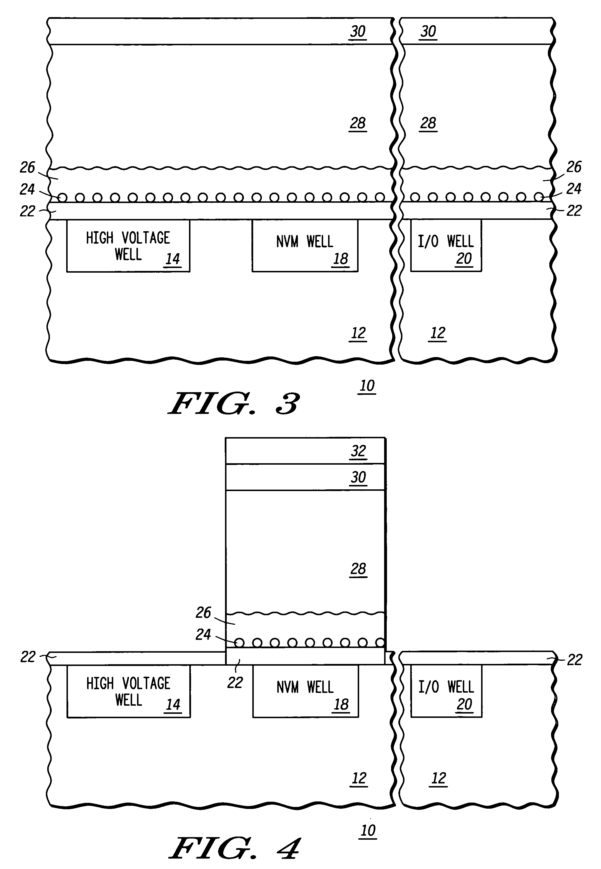
[0012]FIGS. 1–16 show partial side views of a semiconductor wafer during stages in the manufacture of a memory including nanoclusters according to a first embodiment of the present invention. As will be described later, the presently disclosed embodiment utilizes an intermediate dual polysilicon-nitride control electrode stack including a first formed polysilicon-nitride structure and a second formed polysilicon-nitride structure. The second formed polysilicon-nitride structure is removed while periphery device control electrodes are patterned, leaving first formed polysilicon-nitride control electrode structure for the memory cell devices. Such a technique allow...


PUM


Abstract

A plurality of memory cell devices is formed by using an intermediate dual polysilicon-nitride control electrode stack overlying nanoclusters. The stack includes a first-formed polysilicon-nitride layer and a second-formed polysilicon-containing layer. The second-formed polysilicon-containing layer is removed from areas containing the plurality of memory cells. In one form the second-formed polysilicon-containing layer also contains a nitride portion which is also removed, thereby leaving the first-formed polysilicon-nitride layer for the memory cell devices. In another form the second-formed ploysilicon-containing layer does not contain nitride and a nitride portion of the first-formed polysilicon-nitride layer is also removed. In the latter form a subsequent nitride layer is formed over the remaining polysilicon layer. In both forms a top portion of the device is protected from oxidation, thereby preserving size and quality of underlying nanoclusters. Gate electrodes of devices peripheral to the memory cell devices also use the second-formed polysilicon-containing layer.

Description

CROSS-RELATED APPLICATION[0001]This application is related to copending U.S. patent application Ser. No. 10 / 876,805 by Robert F. Steimle entitled “Method of Forming A Nanocluster Charge Storage Device” filed simultaneously herewith and assigned to the assignee of record herein.BACKGROUND[0002]1. Field[0003]The present invention relates to semiconductor devices, and, more particularly, to such devices having nanoclusters.[0004]2. Description of the Related Art[0005]Some devices such as memories (e.g. non volatile memories) utilize discrete charge storage elements called nanoclusters (e.g. of silicon, aluminum, gold, or germanium) for storing charge in a charge storage location of a transistor. In some examples, the nanoclusters are located between two dielectric layers, a bottom dielectric and a control dielectric. Examples of such transistors include thin film storage transistors. A memory typically includes an array of such transistors. Examples of nanocluster types includes doped ...

Claims


Application Information

Patent Timeline
IPC IPC(8): H01L21/302
CPCB82Y10/00H01L21/28273H01L21/28282H01L27/105H01L29/42332H01L27/11546H01L27/11568H01L27/11573H01L27/11526H01L29/40114H01L29/40117H10B41/40H10B41/49H10B43/40H10B43/30
Inventor RAO, RAJESH A.MURALIDHAR, RAMACHANDRANSTEIMLE, ROBERT F.CHINDALORE, GOWRISHANKAR L.
Owner TAIWAN SEMICON MFG CO LTD
Why Eureka
Try Eureka