Embedded dual-port DRAM process

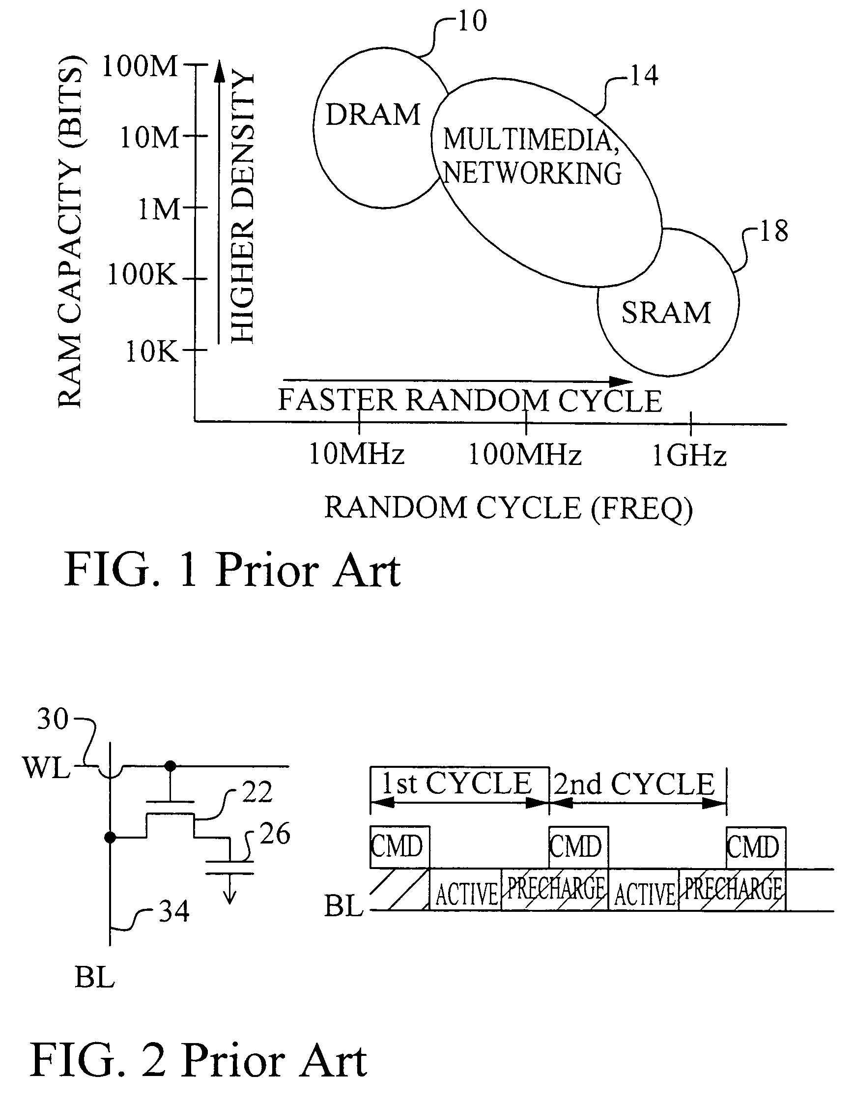
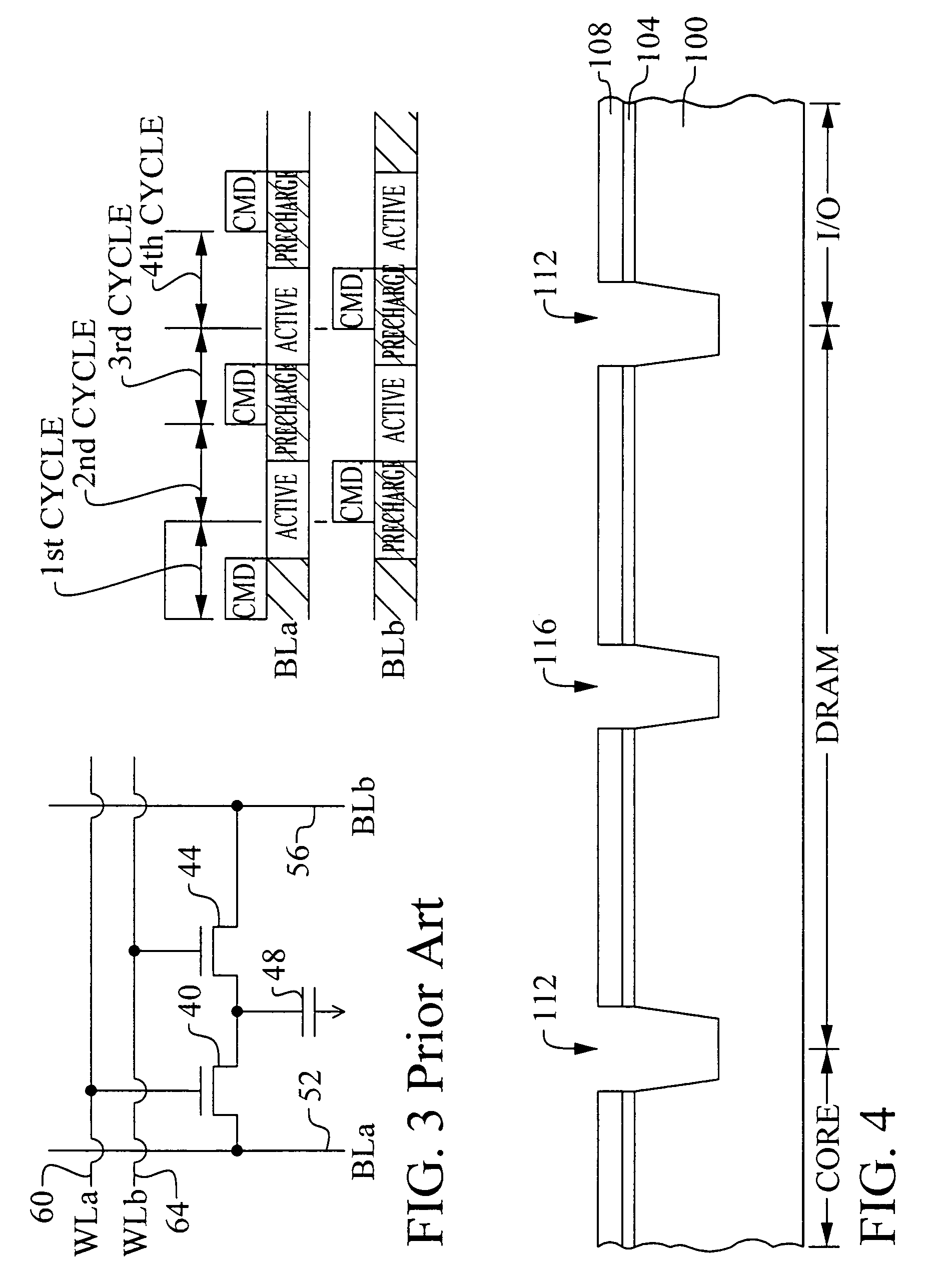
a dual-port dram and process technology, applied in the direction of semiconductor devices, electrical equipment, transistors, etc., can solve the problems of limiting the capacity of dram technologies to about 1 mbit, and the random access operation speed of dram technologies is limited

Inactive Publication Date: 2006-08-15
TAIWAN SEMICON MFG CO LTD
View PDF13 Cites 37 Cited by
  • Summary
  • Abstract
  • Description
  • Claims
  • Application Information

AI Technical Summary

Benefits of technology

[0012]A principal object of the present invention is to provide an effective and very manufacturable method to form dual-port DRAM in an integrated circuit device.
[0014]A yet further object of the present invention is to provide a method to form dual-port DRAM cells having minimal cell area and optimal access speed.
[0016]A yet further object of the present invention is to provide a dual-port DRAM cell having a small layout area and excellent performance.

Problems solved by technology

However, these DRAM technologies are limited in their random access operating speed to the 10 MHz to 100 MHz range.
However, the relatively large cell size of SRAM limits the capacity to about 1 Mbit.

Method used


Image

  • Embedded dual-port DRAM process
  • Embedded dual-port DRAM process
  • Embedded dual-port DRAM process

Examples


Embodiment Construction

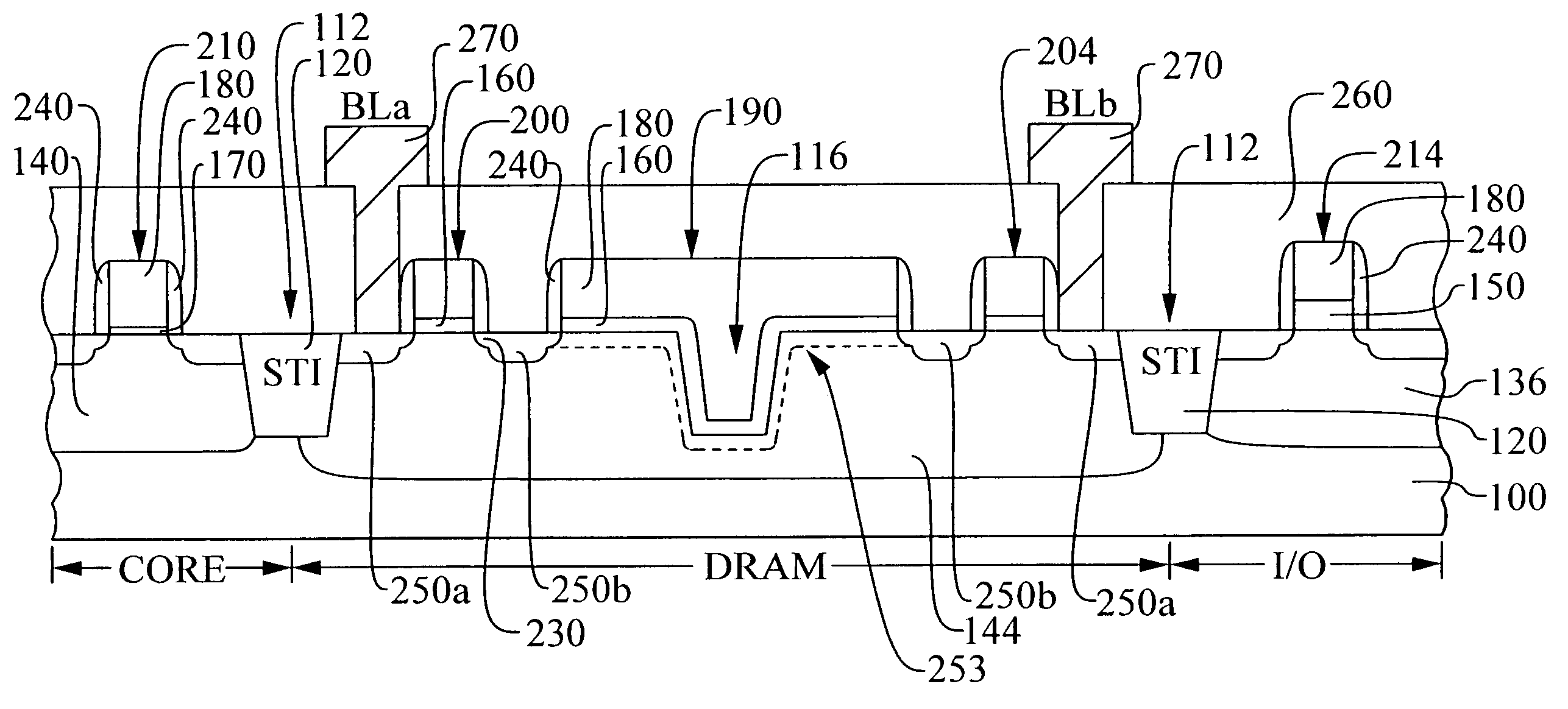
[0025]The preferred embodiments of the present invention disclose a method to form dual-port DRAM cells. The method integrates a unique dual-port DRAM fabrication into a standard CMOS process. It should be clear to those experienced in the art that the present invention can be applied and extended without deviating from the scope of the present invention.

[0026]Referring now to FIGS. 4 through 19, the preferred embodiment of the present invention is illustrated. Many important features of the present invention are shown and discussed below. The preferred embodiment discloses a method to form dual-port DRAM cells in a standard CMOS process. Referring again particularly to FIG. 4, a substrate 100 is provided. The substrate 100 preferably comprises a semiconductor material and, more preferably, comprises monocrystalline silicon. In a process sequence that is typical of widely practice CMOS technology, a pad oxide layer 104 is formed on the substrate wafer 100. Typically, this pad oxide ...


PUM


Abstract

A new method to form DRAM cells in an integrated circuit device is achieved. The method comprises providing a substrate. A plurality of STI regions is formed in the substrate. The STI regions comprise trenches in the substrate. The trenches are filled with a first dielectric layer. All of the first dielectric layer is etched away from a first group of the STI regions to form open trenches while leaving the first dielectric layer in a second group of the STI regions. A second dielectric layer is formed overlying the substrate and lining the open trenches. A conductive layer is deposited overlying the second dielectric layer and completely filling the open trenches. The conductive layer is patterned to define DRAM transistor gates and to define DRAM capacitor top plates. Thereafter, ions are implanted into the substrate to form source and drain regions for the transistors.

Description

[0001]This application is a divisional of 10 / 438,646 May 15, 2003 U.S. Pat. No. 6,794,254.BACKGROUND OF THE INVENTION[0002](1) Field of the Invention[0003]The invention relates to an integrated circuit memory device, and, more particularly, to a method to form dual-port DRAM cells in an integrated circuit device.[0004](2) Description of the Prior Art[0005]Modern multimedia applications and personal computers require large RAM memory systems with high throughput rates. In particular, three-dimensional graphics rendering and networking applications demand a combination of fast random access cycle times, low latency, and large memory sizes.[0006]Referring now to FIG. 1, a plot is shown of typical RAM capacities (bits) versus random access cycle frequency (Hz). It is found that the largest capacities can be formed in dynamic RAM (DRAM) technologies 10. However, these DRAM technologies are limited in their random access operating speed to the 10 MHz to 100 MHz range. It is also found tha...

Claims


Application Information

Patent Timeline
Patent Type & Authority Patents(United States)
IPC IPC(8): H01L27/108H01L21/336H01L21/8242
CPCH01L27/10894H01L27/1087H10B12/0387H10B12/09
Inventor TZENG, KUO-CHYUANCHIANG, MING-HSIANGCHIANG, WEN-CHUANSINITSKY, DENNIS J.
Owner TAIWAN SEMICON MFG CO LTD
Why Eureka
Try Eureka