Novel embedded dual-port DRAM process
- Summary
- Abstract
- Description
- Claims
- Application Information
AI Technical Summary
Benefits of technology
Problems solved by technology
Method used
Image
Examples
Embodiment Construction
[0024] The preferred embodiments of the present invention disclose a method to form dual-port DRAM cells. The method integrates a unique dual-port DRAM fabrication into a standard CMOS process. It should be clear to those experienced in the art that the present invention can be applied and extended without deviating from the scope of the present invention.
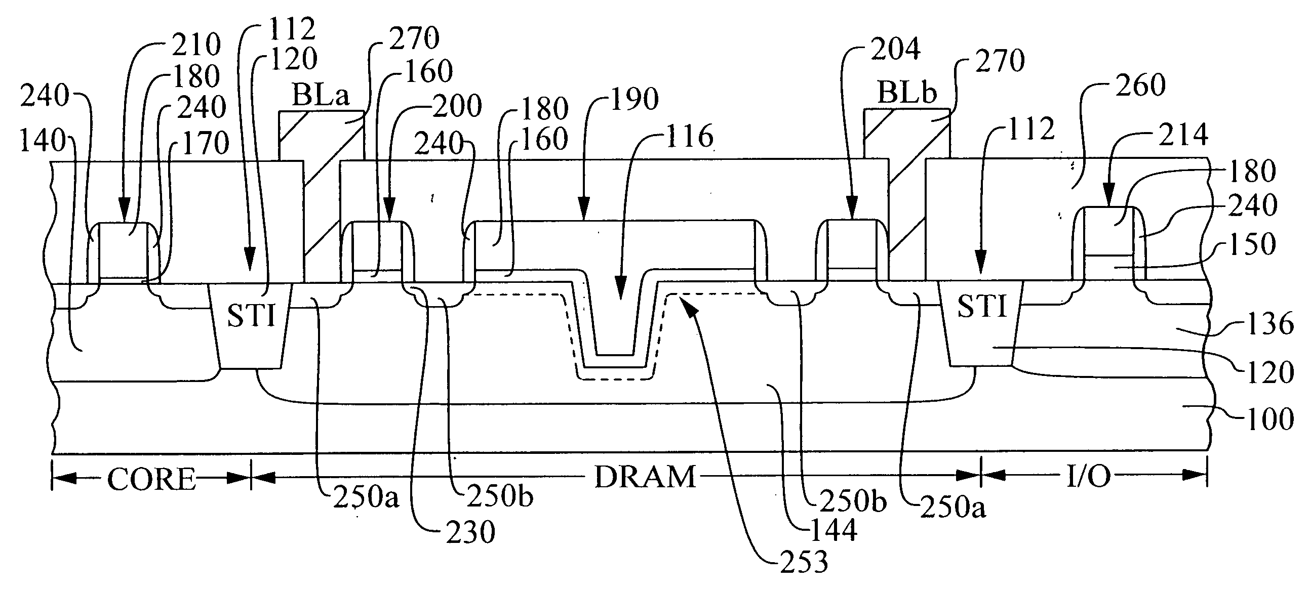
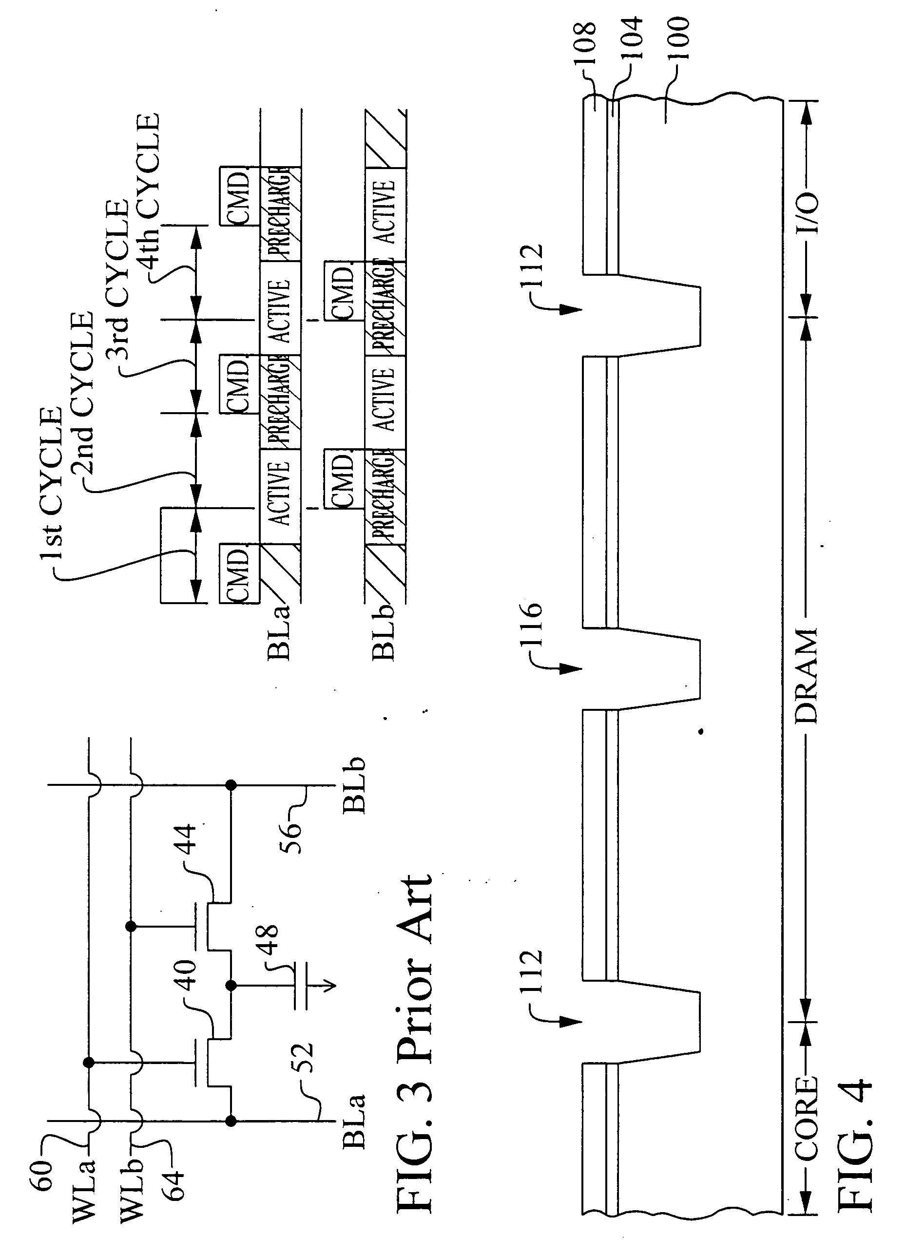
[0025] Referring now to FIGS. 4 through 19, the preferred embodiment of the present invention is illustrated. Many important features of the present invention are shown and discussed below. The preferred embodiment discloses a method to form dual-port DRAM cells in a standard CMOS process. Referring again particularly to FIG. 4, a substrate 100 is provided. The substrate 100 preferably comprises a semiconductor material and, more preferably, comprises monocrystalline silicon. In a process sequence that is typical of widely practice CMOS technology, a pad oxide layer 104 is formed on the substrate wafer 100. Typically, this pad oxi...
PUM
 Abstract
Description
Claims
Application Information


