Electronic circuit device

a technology of electronic circuit device and integrated circuit, which is applied in the direction of error detection/correction, radio frequency controlled devices, instruments, etc., can solve the problems of long development time, disadvantageous to responding quickly to market demands, and performance encountering design complexity, etc., to achieve high-speed memory access and precise response to the demand of speed-up

Inactive Publication Date: 2006-08-15
RENESAS TECH CORP
View PDF12 Cites 74 Cited by
  • Summary
  • Abstract
  • Description
  • Claims
  • Application Information

AI Technical Summary

Benefits of technology

[0019]This electronic circuit device, which is based on the organic combination of the MCM, FPGA and FPMC techniques, facilitates the debugging at early stages of SOC-based system development without imposing operational speed and noise problems, and is also useful for the configuration of a prototype system. It contributes to the time reduction throughout the system development, prototype fabrication and large-scale production. The electronic circuit device, when it is intended to be a commercial product to replace a SOC-based LSI, is advantageous overwhelmingly in terms of cost reduction, particularly in the case of small-quantity large-variety production, and it is comparable to SOC in terms of performance and board size.
[0036]It is possible for the electronic circuit device with the provision of the JTAG-based test function to adopt the high-density mount board structure of the build-up board. The semiconductor devices may be each equipped with a microcomputer with CPU and a random access memory, with the microcomputer being adapted to connect to the external mounting pins. If the microcomputer incorporates a first electrically-rewritable nonvolatile memory which can store the operation program of CPU, it becomes possible to simulate on a software basis the function to be realized by the electronic circuit device. By the provision of the microcomputer with a memory buffer, which is connected to the random access memory through the exclusive memory bus, it is possible to speed up the memory access as in the case described previously. Arranging the output circuit of memory buffer so as to be variable in output impedance, as in the previous case, facilitates the impedance matching with the exclusive memory bus. Moreover, using the above-mentioned programmable device as one of semiconductor devices facilitates the hardware-based simulation of the function to be realized by the electronic circuit device.<Externally Attached Programmable Device>

Problems solved by technology

Semiconductor integrated circuit devices (LSI) which are amid the trends of enhancement in integration density and performance are encountering the design complexity.
The longer development time is disadvantageous to responding quickly to market demands.
However, such a scheme is yet to be offered.
Firstly, the separate use of MCM and FPGA necessitates a larger board for mounting them and a longer wiring, and consequently in some cases does not behave the intended characteristics for implementing the function equivalent to an SOC-based LSI.

Method used


Image

  • Electronic circuit device
  • Electronic circuit device
  • Electronic circuit device

Examples


first embodiment

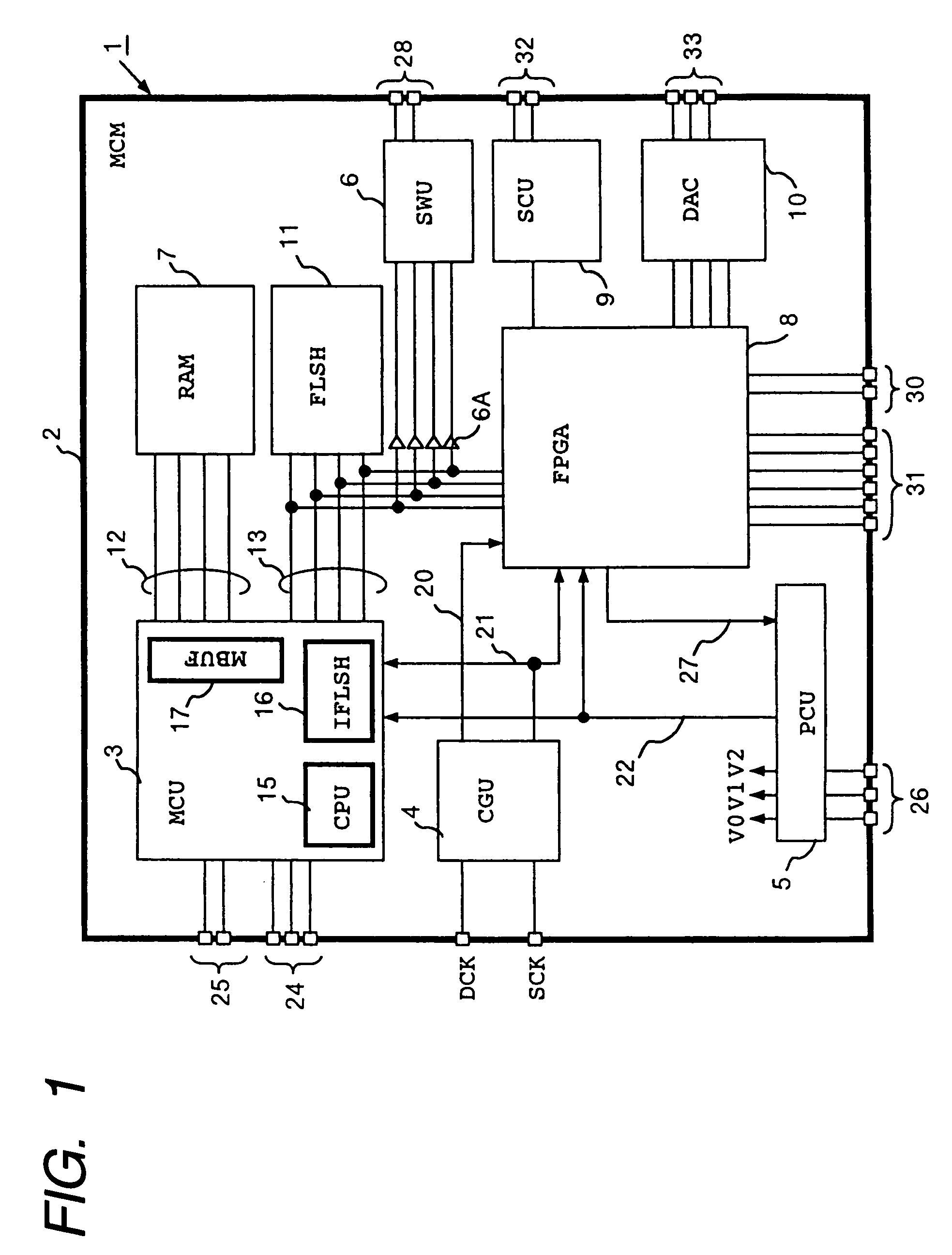
[0059]FIG. 1 shows an MCM 1 which is the inventive electronic circuit. This MCM 1 is intended in this example for the application to a system that is oriented to graphic control inclusive of display, imaging and data compression, although this affair is not compulsory.

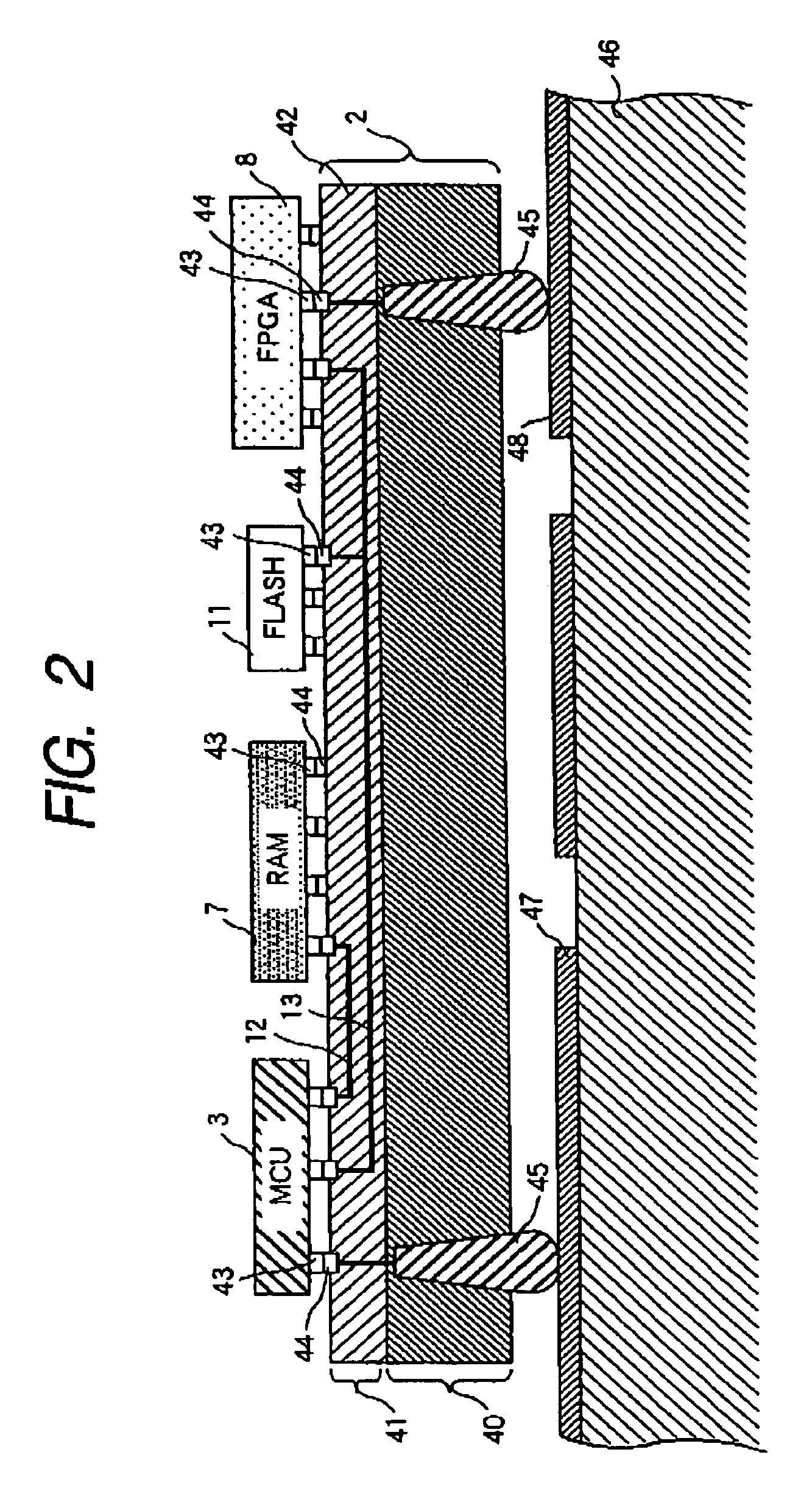
[0060]The MCM1 includes semiconductor devices formed on one side of a high-density mount board 2, which are a microcomputer (MCU) 3, clock generation unit (CGU) 4, power control unit (PCU) 5, switch unit (SWU) 6, random access memory (RAM) 7, programmable device (FPGA) 8, serial communication unit (SCU) 9, digital-to-analog converter (DAC) 10, and flash memory (FLSH) 11. The random access memory 7 is connected to the microcomputer 3 through an exclusive memory bus 12. The microcomputer 3, FPGA 8 and flash memory 11 share a common system bus 13.

[0061]The CGU 4 having inputs of a system clock signal SCK and display clock signal DCK multiplies or demultiplies the frequencies of these clock signals to release a resulting d...

second embodiment

[0104]FIG. 6 shows an MCM 1A which is the inventive electronic circuit. This MCM 1A differs from the MCM 1 shown in FIG. 1 in the adoption of an MCU 3A which does not have the on-chip flash memory 16. The MCU is generally designed to incorporate the flash memory in case the high-speed operation of flash memory is intended or in case the confinement of high secrecy data within the LSI chip is intended. If these cases are not relevant, it is enough to use the MCU 3A without a flash memory.

[0105]Another elimination is the SWU 6 and PCU 5, and the operational power voltages V0, V1 and V2 are supplied directly from the outside. The program-end signal 27 is released from the mount board 2A to the outside, and the system reset signal 22 is given from the outside of the board 2A. The rest is the same as the preceding one shown in FIG. 1, and further explanation is omitted.

third embodiment

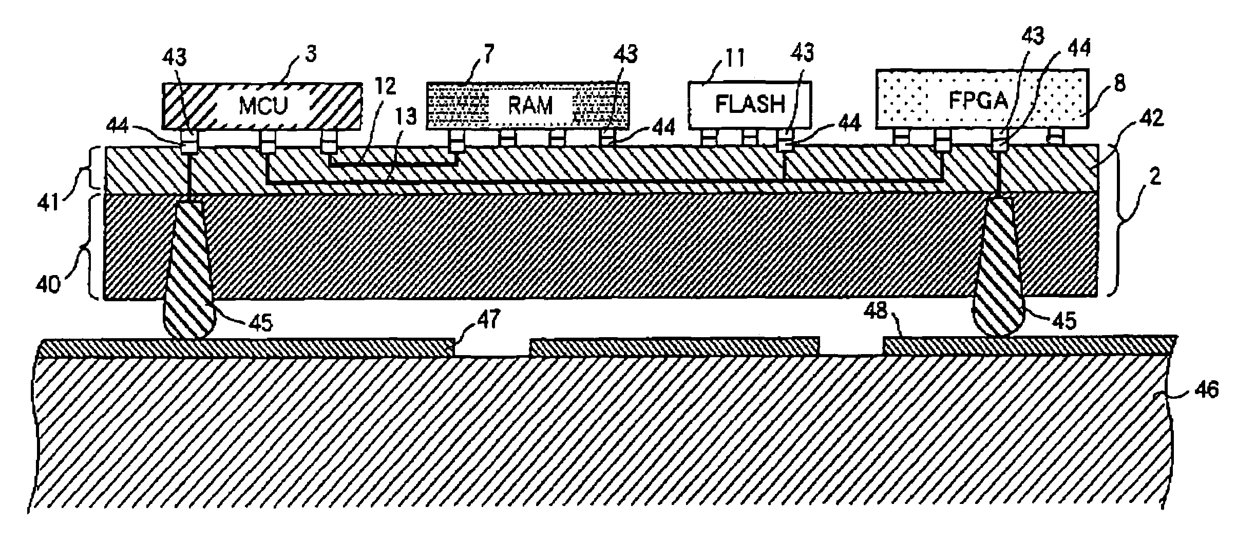
[0106]FIG. 7 shows an MCM 1B which is the inventive electronic circuit. This MCM 1B differs from the MCM 1 shown in FIG. 1 in the external connection of the flash memory 11 outside of the mount board 2B. The flash memory 11 and MCM 1B are mounted on the mother board 46. The flash memory is generally very slow in access speed relative to the memory bus, and therefore it can be outside of the mount board 2B unless otherwise required by the application system. Moreover, in case a significant difference in the storage capacity of the flash memory 11 depending on the application is anticipated, it is advantageous to have the flash memory 11 outside of the mount board 2 so as to gain the system flexibility.

[0107]Another elimination is the SWU 6 and PCU 5, and the operational power voltages V0, V1 and V2 are supplied directly from the outside. The program-end signal 27 is released from the mount board 2B to the outside, and the system reset signal 22 is given from the outside of the board ...


PUM


Abstract

An electronic circuit device has a high-density mount board, on which are disposed a microcomputer, a random access memory, a programmable device which is a variable logic circuit represented by FPGA, and an electrically-rewritable nonvolatile memory which can store the operation program of the microcomputer. The high-density mount board has external mounting pins on the bottom surface so as to be mounted on a mother board in the same manner as a system on-chip multi-chip module. With an intended logic function being set on the programmable device, a hardware-based function to be realized by the electronic circuit device is simulated. With an operation program being written to the nonvolatile memory, a software-based function to be realized is simulated. Consequently, the device facilitates the debugging at early stages of system development, configures a prototype system, and contributes to the time reduction throughout the system development, prototype fabrication and large-scale production.

Description

[0001]This application is a PCT Application Number PCT / JP01 / 00326 filed on Jan. 19, 2001, which designates the United States, and claims priority therefrom under 35 U.S.C. § 120.TECHNICAL FIELD[0002]The present invention relates to an electronic circuit device having MCM (Multi-Chip Module) structure, and to a technique which is applicable effectively to, for example, an electronic circuit device used for the debugging at early stages of SOC (System On Chip) or MCM-oriented system development and also for the configuration of a prototype system.BACKGROUND ART[0003]Semiconductor integrated circuit devices (LSI) which are amid the trends of enhancement in integration density and performance are encountering the design complexity. For an LSI user who plans to develop an application system, it will take in many cases as long as one year before having a complete LSI. The longer development time is disadvantageous to responding quickly to market demands. In order to reduce the development...

Claims


Application Information

Patent Timeline
Patent Type & Authority Patents(United States)
IPC IPC(8): H01L23/52G06F11/267G06F15/78
CPCG06F11/261G06F11/267G06F15/7867H01L25/18H01L2924/09701H01L2924/3011H01L2924/13091H01L2224/16225H01L2924/15192H01L2924/15311H01L2924/00H01L2924/00014H01L2224/0401
Inventor FUJITA, RYOKUBO, OSAMUNOGUCHI, KOUKIKUBO, MASAHARUMISHIMA, MICHIHIROTAKAHASHI, YASUHIKO
Owner RENESAS TECH CORP
Why Eureka
Try Eureka