Crack resistant scribe line monitor structure and method for making the same

a monitor and scribe line technology, applied in the direction of semiconductor/solid-state device testing/measurement, semiconductor device details, semiconductor/solid-state device testing/measurement, etc., can solve the problems of low k dielectric materials that are easy to be damaged, low k dielectric materials are difficult to handle than traditionally employed higher k materials,

Active Publication Date: 2006-08-15
ADVANCED MICRO DEVICES INC
View PDF6 Cites 9 Cited by
  • Summary
  • Abstract
  • Description
  • Claims
  • Application Information

AI Technical Summary

Benefits of technology

[0005]There is a need for providing a structure and methodology for making the same that prevents or

Problems solved by technology

There are a number of concerns in using low k materials, such as being more difficult to handle than traditionally employed higher k materials, such as oxides.
Also, low k dielectric materials are readily damaged by techniques used to remove photoresist materials after the patterning of a layer.
Another problem with low k dielectric materials, especially porous low k dielectric materials, is their relatively low mechanical strength.
This can lead to a number of concerns in the final product, since a relatively low mechanical strength makes the low k materials susceptible to delamination and scratching during

Method used


Image

  • Crack resistant scribe line monitor structure and method for making the same
  • Crack resistant scribe line monitor structure and method for making the same
  • Crack resistant scribe line monitor structure and method for making the same

Examples


Embodiment Construction

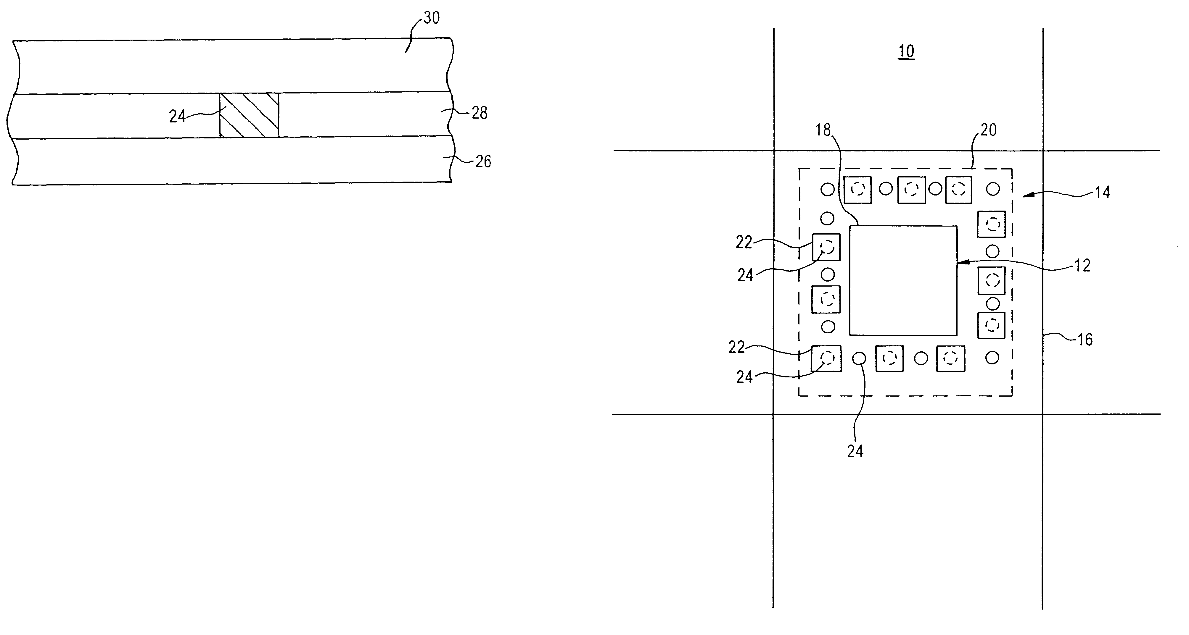
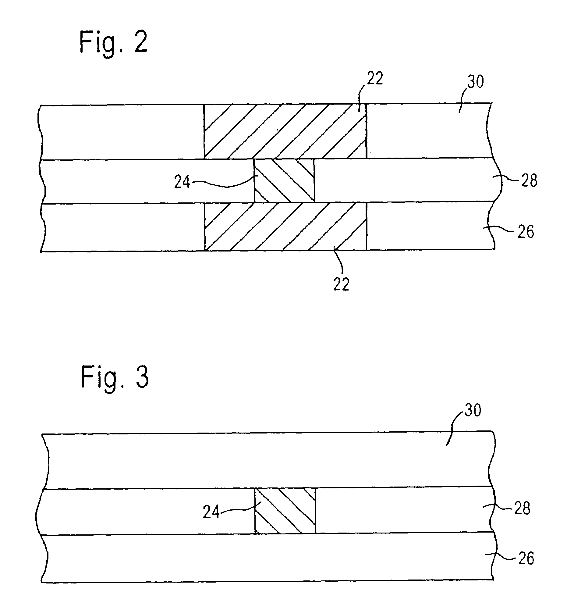
[0016]The present invention addresses problems related to the propagation of cracks during sawing or die mishandling after a saw process has been performed. These cracks can propagate to the main die area, and are especially prevalent in devices employing low k dielectric layers, possibly due to low k dielectric adhesion to metals.

[0017]These problems are solved, in part, by the present invention which provides for stress relief elements or crack stop elements, provided in a scribe line monitor area that circumferentially surrounds the main die area. These stress relief elements or crack stop elements, in the form of dummy vias, for example, serve to make the scribe line monitor area crack resistant so that cracks do not propagate, during sawing or post-saw handling, to the main die area. This increases the yield and reliability of the final product.

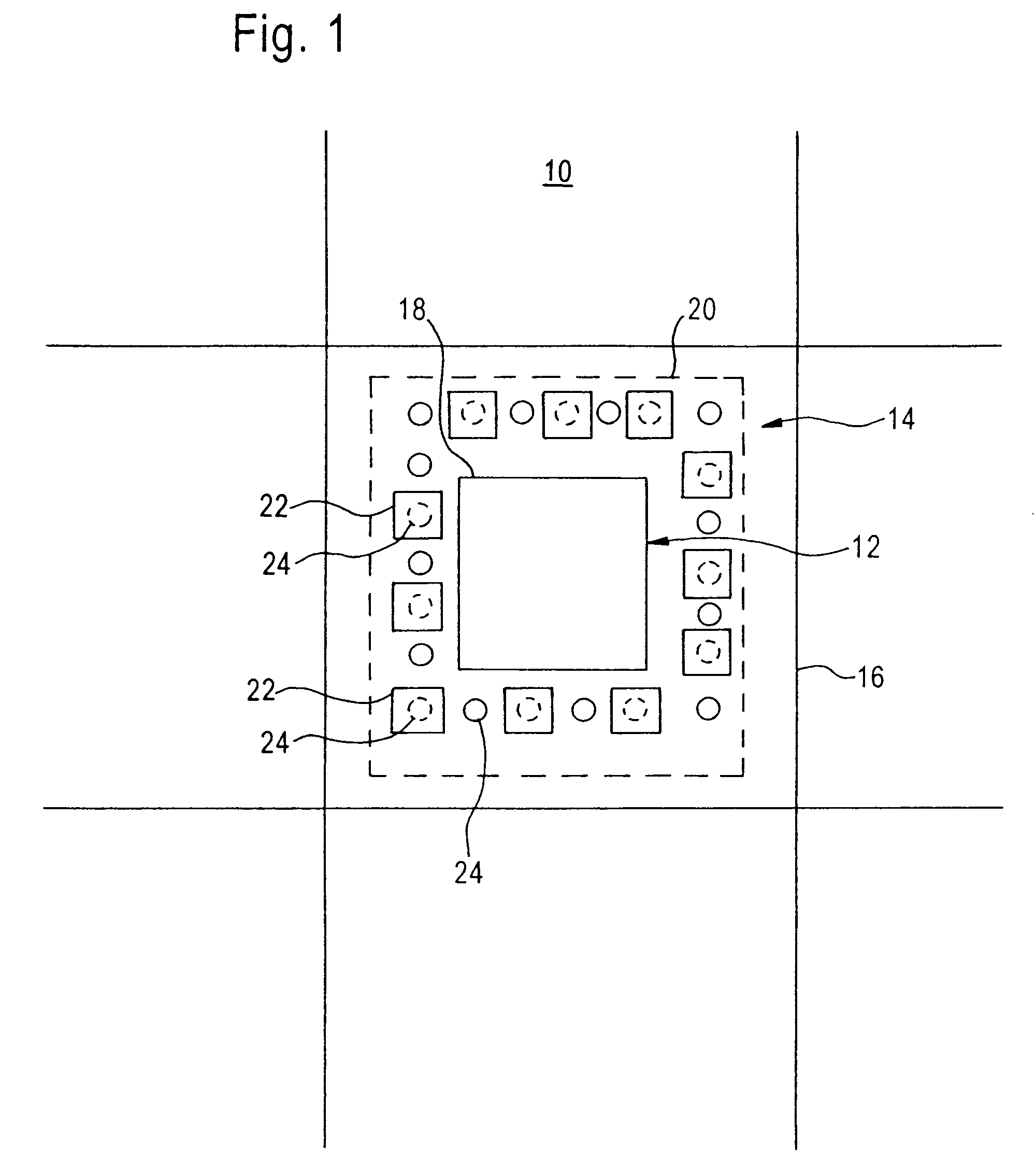
[0018]FIG. 1 depicts a top view of a portion of a semiconductor wafer 10 which is formed in accordance with embodiments of the present ...


PUM


Abstract

A method and structure prevents crack propagation to the active die circuitry of a main die area during sawing around the outer periphery of the main die area. Stress relief elements, such as dummy vias, are provided in the scribe line area between the saw lane and the main die area. The dummy vias prevent cracks induced by the sawing process from propagating to the main die area.

Description

FIELD OF THE INVENTION[0001]The present invention relates to the field of semiconductor device fabrication, and more particularly, to the separation of semiconductor devices from a semiconductor wafer.BACKGROUND OF THE INVENTION[0002]In efforts to improve the operating performance of a chip, low k dielectric materials have been increasingly investigated for use as replacements for dielectric materials with higher k values. Lowering the overall k value of the dielectric layer employed in the metal interconnect layers lowers the RC of the chip and improves its performance. There are a number of concerns in using low k materials, such as being more difficult to handle than traditionally employed higher k materials, such as oxides. Also, low k dielectric materials are readily damaged by techniques used to remove photoresist materials after the patterning of a layer. Another problem with low k dielectric materials, especially porous low k dielectric materials, is their relatively low mec...

Claims


Application Information

Patent Timeline
IPC IPC(8): H01L23/48H01L23/52H01L29/40
CPCH01L21/78H01L22/34H01L23/562H01L23/585H01L2924/0002H01L2924/00
Inventor EPPES, DAVID H.
Owner ADVANCED MICRO DEVICES INC
Why Eureka
Try Eureka