Computer aided design method and apparatus for modeling and analyzing on-chip interconnect structures

a computer-aided design and interconnect structure technology, applied in the field of circuit design systems, can solve the problems of complicating circuit design, inability to accurately characterization wide-band electrical circuits of high-performance electrical interconnect structures, etc., and achieve the effect of optimal circuit performance and facilitate electrical circuit interconnect design

Inactive Publication Date: 2006-08-15
INT BUSINESS MASCH CORP
View PDF7 Cites 31 Cited by
  • Summary
  • Abstract
  • Description
  • Claims
  • Application Information

AI Technical Summary

Benefits of technology

[0011]It is yet another purpose of the invention to provide IC designers with the most accurate semiconductor process parameter descriptions;

Problems solved by technology

These lump values at best provide rule of thumb design guidance and do not lend themselves to accurate wide-band electrical circuit characterizations of high-performance electrical interconnect structures.
This complicates circuit design because in addition to active element models that are accurate over the expected operating frequency range, either the circuit model must somehow accommodate wide-band models for on-chip conductors or different conductor models must be employed at each of a number of points across the frequency spectrum to accommodate the full range of conductor characteristics.

Method used


Image

  • Computer aided design method and apparatus for modeling and analyzing on-chip interconnect structures
  • Computer aided design method and apparatus for modeling and analyzing on-chip interconnect structures
  • Computer aided design method and apparatus for modeling and analyzing on-chip interconnect structures

Examples


Embodiment Construction

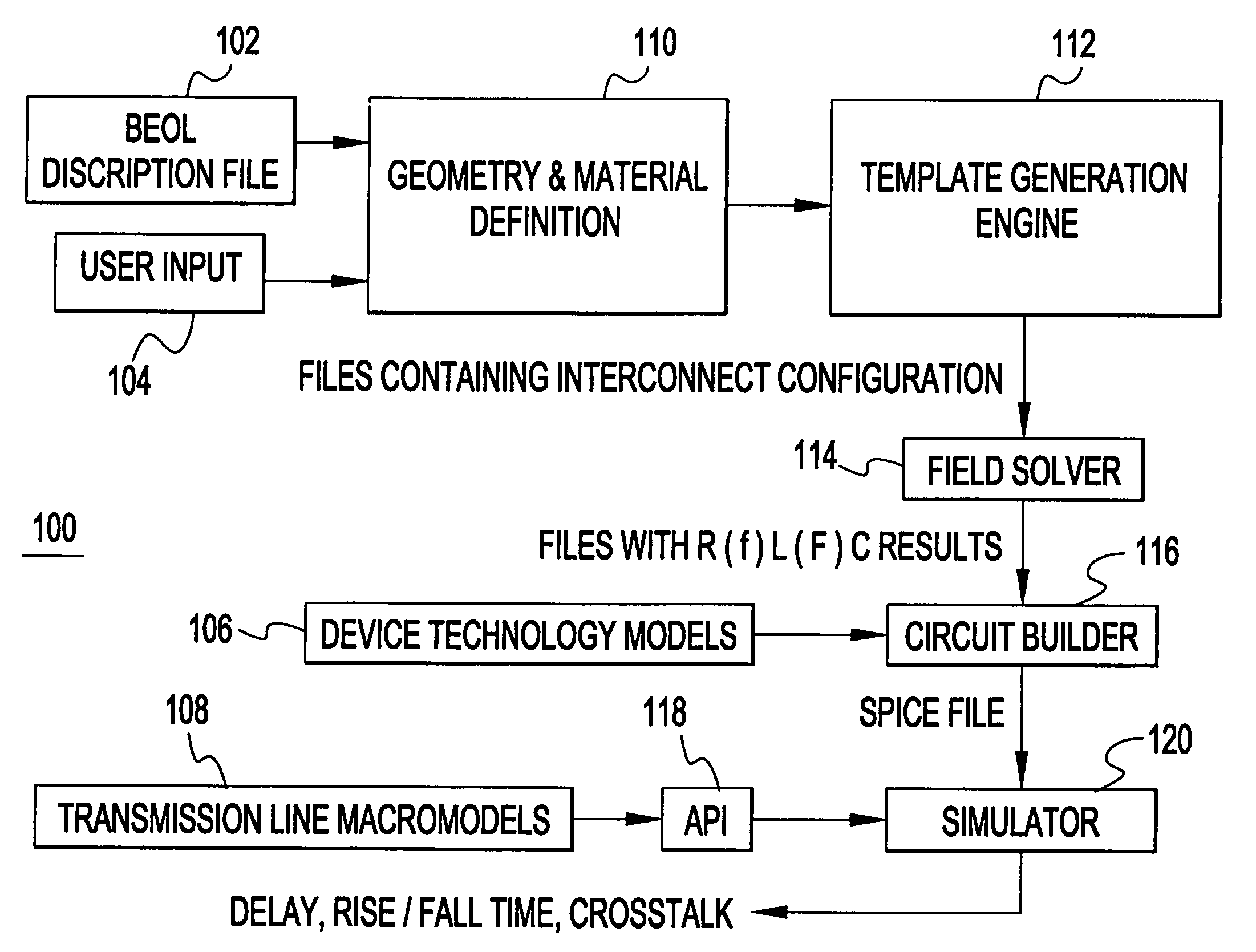
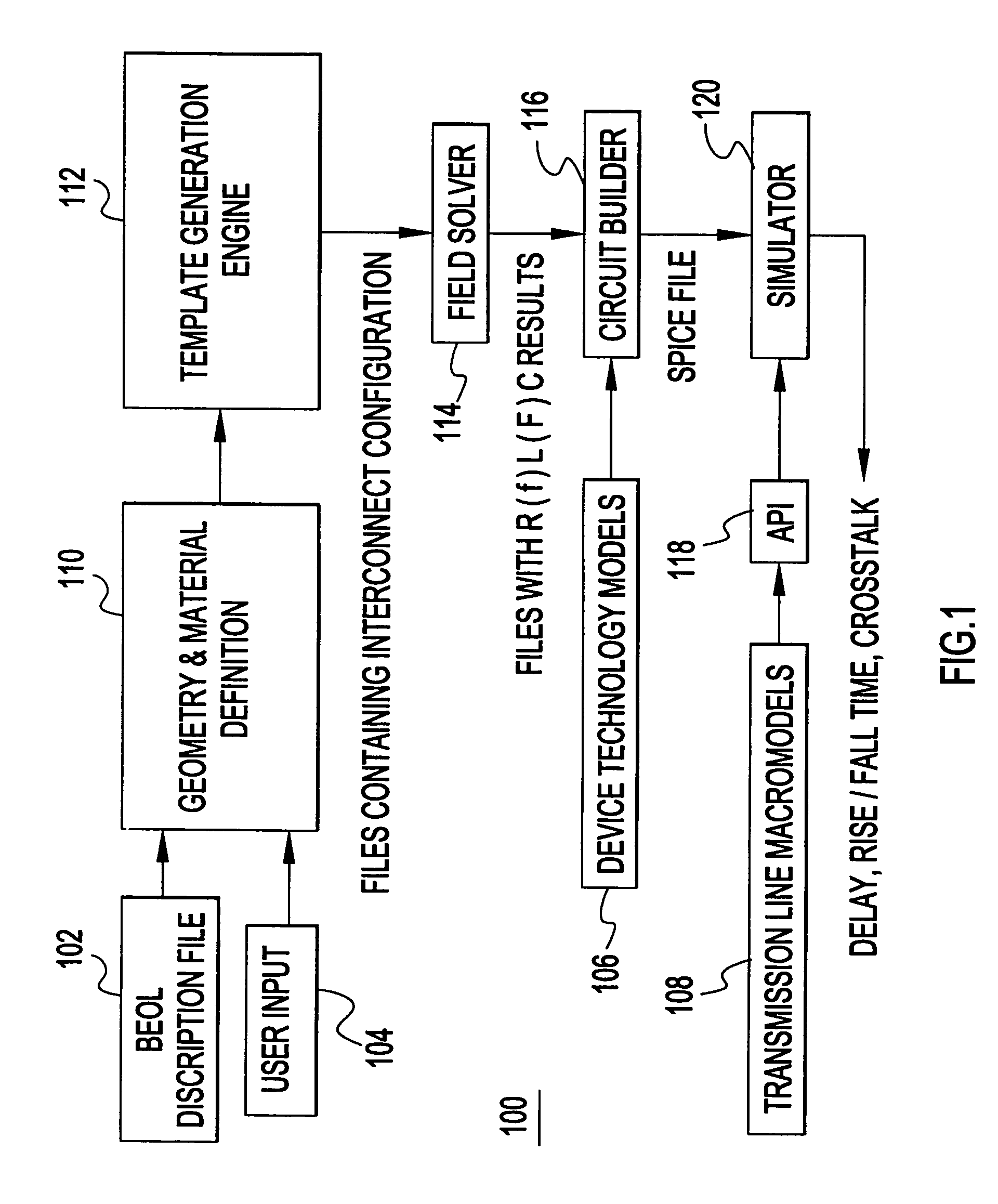
[0023]Turning now to the drawings and, more particularly, FIG. 1 shows a block diagram of an example of a fully automated computer aided design (CAD) system 100 with wide-band characterization of on-chip interconnect structures according to a preferred embodiment of the present invention. As with any state of the art CAD system, a preferred embodiment system runs on a typical state of the art general purpose computer, such as for example a main frame computer, a scientific workstation, or a suitably equipped personal computer. Similarly, CAD modules may be distributed over a number of computers, each running one or more design module and the data files, such as for example, process parameter data and the like. The data files may be stored locally, e.g., on a personal computer, or stored remotely on a server with the process data being provided to, and being accessed by, individual modules as required. Further, a general purpose computer, main frame computer server, scientific workst...


PUM


Abstract

A computer aided design (CAD) system. A template generation engine generates templates from interconnect configuration files. A field solver generates high frequency passive element relationships from the templates. A circuit builder generates circuit description files from device technology models and from high frequency passive element relationships. Parameterized circuit description models may be generated for large range of sensitivity analyses. A simulator simulates circuit responses for transmission line models from the circuit description files. Interconnect configuration files may be generated by a geometry and material definition module that receives process description data from a designer.

Description

BACKGROUND OF THE INVENTION[0001]1. Field of the Invention[0002]The present invention is related to circuit design systems and more particularly to computer aided design (CAD) systems for designing integrated circuits (ICs) operating over a wide frequency band and with circuit interconnects that might experience transmission line effects.[0003]2. Background Description[0004]Sets of software programs are well known in the art as computer aided design (CAD) tools. Typical CAD tools include automatic layout tools, timing analysis tools, logic synthesis tools, and so forth. In addition, a CAD tool may include electromagnetic (EM) field solvers (also known as parameter extractors) and circuit simulators for circuit conductor (interconnect) analysis and design. Integrated circuit (IC) designers have found CAD tools invaluable for designing, analyzing and verifying complex ICs and IC chip designs, such as microprocessors, microcontrollers, communications circuits and the like.[0005]Providi...

Claims


Application Information

Patent Timeline
Patent Type & Authority Patents(United States)
IPC IPC(8): G06F17/50G06F9/455G06F19/00G06G7/62
CPCG06F17/5036G06F30/367
Inventor ANAND, MINAKSHISUNDARAN B.ANGYAL, MATTHEW S.DEUTSCH, ALINAELFADEL, IBRAHIM M.KOPCSAY, GERARD V.RUBIN, BARRY J.SMITH, HOWARD H.
Owner INT BUSINESS MASCH CORP
Why Eureka
Try Eureka