Method and arrangement for a power amplifier
- Summary
- Abstract
- Description
- Claims
- Application Information
AI Technical Summary
Benefits of technology
Problems solved by technology
Method used
Image
Examples
first embodiment
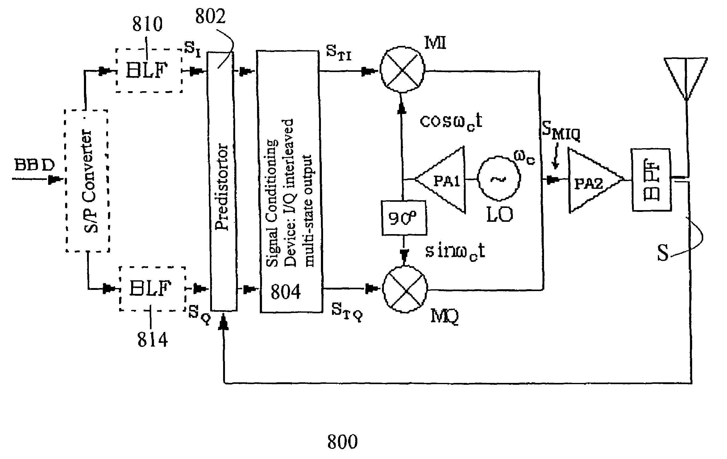
[0032]In FIG. 3, the present invention is shown. The multiplexing device is implemented by means of multiplier devices MI and MQ, a phase shifter 302 and a Local Oscillator (LO). The LO generates the carrier wave with the frequency ωc and the phase shifter shifts the phase of the carrier wave 90 degrees. Here, the output signals SMIQ from the devices MI and MQ, which are controlled by STI and STQ respectively, will not overlap in time with each other, since the two multiplier devices MI and MQ are never enabled at the same time. If STI is separated from zero then STQ is always zero and visa-versa. Thus, the RF signal SMIQ from the devices MI and MQ, may be a high-power RF signal and a Pulse-Width Modulated (PWM) signal, as shown in FIG. 4.
Pulse-Width Modulated Signal
[0033]FIG. 4 shows the PWM signals STI (on the I-axis) and STQ (on the Q-axis). The STI and STQ PWM signals have the states of +1, 0, −1 (n=3).[0034]STI=+1:
[0035]When the STI channel is in +1 state, then an RF carrier is...
second embodiment
[0047]In FIG. 5, the present invention shows a possible approach of implementing the MI and MQ multiplier devices by using tri-state switches. Here, the switching frequency for respective device MI and MQ, controlled by respective signal, STI and STQ, is in the order of several hundreds of MHz, depending on the bandwidth of the baseband signal which is usually on the order of a few tens of MHz. At these operating frequencies, semiconductor mixers and switches are readily available. It is also shown in FIG. 5 that the amplification of the RF signals can be split between two different amplifiers PA1, PA2. This implies that the normal low-level power carrier wave, with the frequency ωc generated by the LO first is amplified by using a high-efficient NLPA PA1. This is possible because the carrier wave ideally is an unmodulated sine wave that can be amplified by an NLPA without causing problems of generating intermodulation products. Depending on available power-handling capability of sw...
third embodiment
[0048]Further, in an amplifier device 600 shown in FIG. 6, only one multi-throw switch MC is used to perform the required PWM of a, e.g. multiphase, signal. The number of throws in the switch is herein referred to as n. To control the switch, it is required by the SCD 602 to generate a five-state (n=5) control signal Sc, (because of the five throw switch), as shown in the present invention in FIG. 6. Sc is a five state control line (digital signal) that controls which RF phase shift (or null signal), that is sent to the power amplifier PA2. In order to generate the control signal Sc, the two three-state outputs from the SCD, i.e. STI and STQ showed in the previous embodiments, may be passed into a signal translation unit (not shown in the drawings), with Sc as the output signal. The signal translation unit has the following function:
[0049]
STISTQSC00 0 degrees (MC is in the top position, see FIG. 6.)0−1270 degrees (MC is in the second position down.)−10180 degrees (MC is in the third...
PUM
 Abstract
Description
Claims
Application Information


