Method and apparatus for high-speed thickness mapping of patterned thin films
a technology of patterned thin films and thickness mapping, which is applied in the field of film thickness measurement, can solve the problems of affecting the efficiency of semiconductor manufacturing, and requiring substantial space in the semiconductor fabrication cleanroom. the rate of semiconductor processing is too slow, and the system is too slow to be used concurrently with semiconductor processing
- Summary
- Abstract
- Description
- Claims
- Application Information
AI Technical Summary
Benefits of technology
Problems solved by technology
Method used
Image


Examples
examples
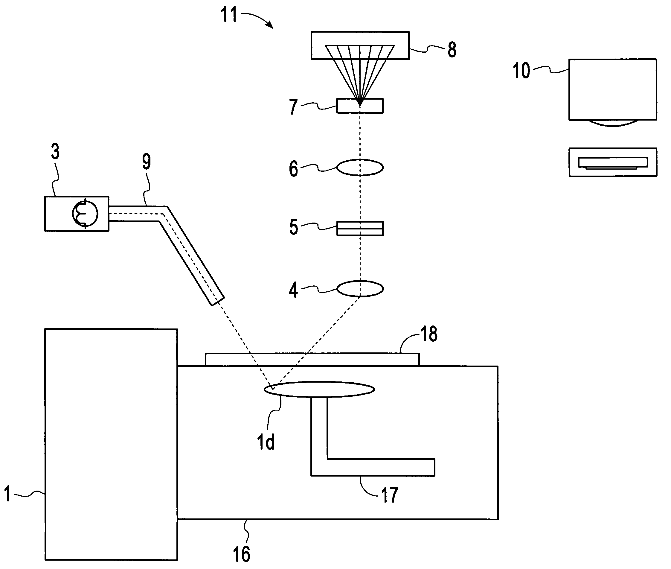
[0046]In an example embodiment of the subject invention, suitable for use in a CVD environment, the light source 3 is a tungsten / halogen regulated light source, manufactured by Stocker & Yale, Inc., Salem, N.H.
[0047]Fiber / fiber bundle 9 in this embodiment is a bundle configured into a line of fibers to provide uniform illumination along the measured surface. Such a fiber optic “line light” is manufactured by several companies, Stocker & Yale being a prime example.
[0048]This example is configured for use with CVD processing system Model P5000 manufactured by Applied Materials Inc., Santa Clara, Calif. An optically clear viewport 18 is provided in the standard P5000 configuration.
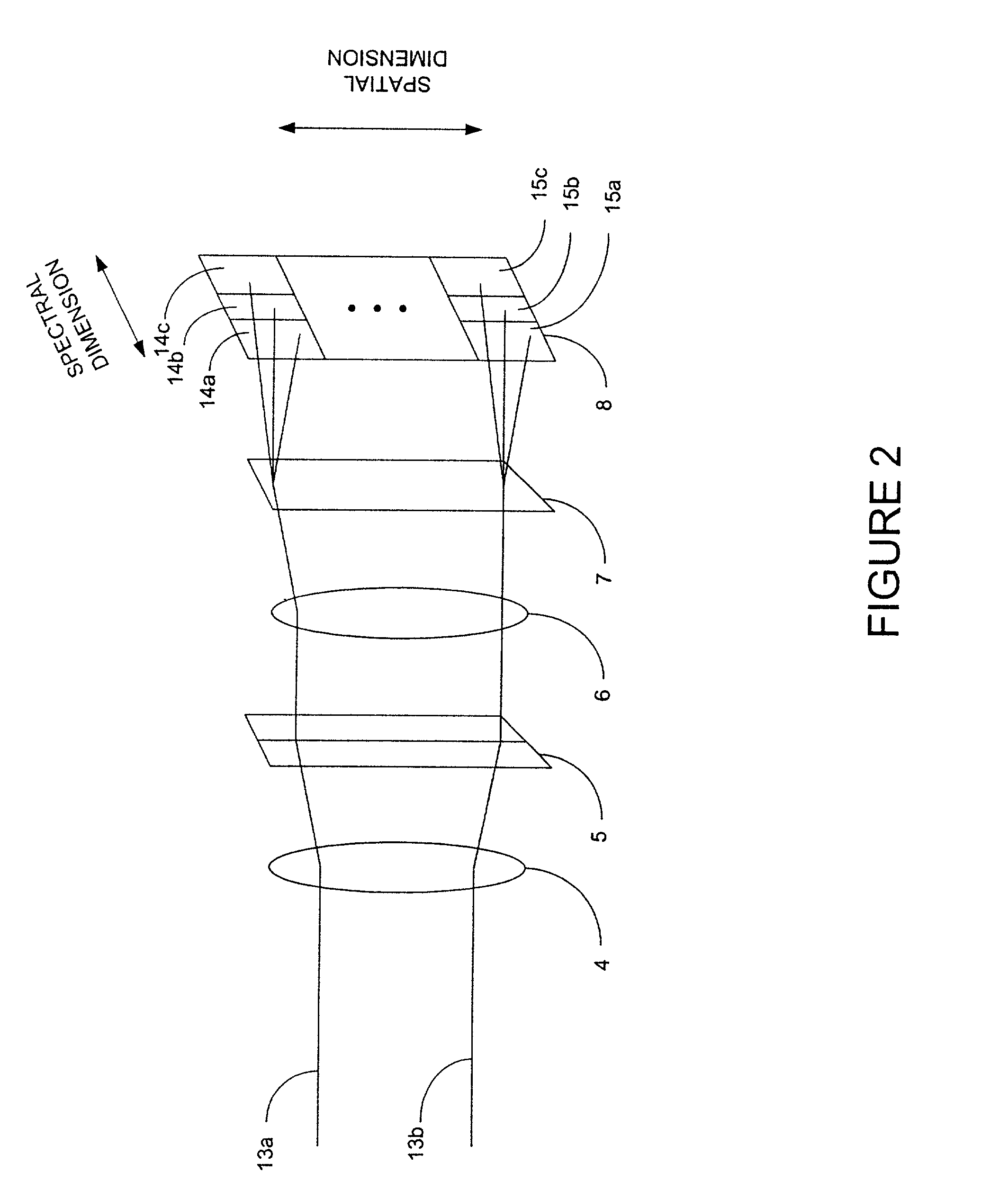
[0049]The line imaging spectrometer 11 in this example is manufactured by Filmetrics, Inc., San Diego, Calif., the assignee of the subject application. In this spectrometer, the imager 8 is a CCD imager incorporating a time delay and integration line scan camera manufactured by Dalsa Inc., Part No. CT-E4-2048...
PUM
| Property | Measurement | Unit |
|---|---|---|
| thick | aaaaa | aaaaa |
| thickness | aaaaa | aaaaa |
| thickness | aaaaa | aaaaa |
Abstract
Description
Claims
Application Information
 - R&D
- Intellectual Property
- Life Sciences
- Materials
- Tech Scout
- Unparalleled Data Quality
- Higher Quality Content
- 60% Fewer Hallucinations
Browse by: Latest US Patents, China's latest patents, Technical Efficacy Thesaurus, Application Domain, Technology Topic, Popular Technical Reports.
© 2025 PatSnap. All rights reserved.Legal|Privacy policy|Modern Slavery Act Transparency Statement|Sitemap|About US| Contact US: help@patsnap.com