System and methods for connecting electrical components

a technology of electrical components and systems, applied in the direction of connection contact material, coupling device connection, conductive pattern formation, etc., can solve the problems of increasing the size and power of electrical circuits and components, increasing the number of individual connectors, and increasing the number of electrical components

Inactive Publication Date: 2006-08-29
METHODE ELETRONICS INC
View PDF55 Cites 19 Cited by
  • Summary
  • Abstract
  • Description
  • Claims
  • Application Information

AI Technical Summary

Problems solved by technology

Regardless of the type of electrical system, advances in technology have led electronic circuits and components to become increasingly smaller and more powerful.
However, individual connectors are still, in general, relatively large compared to the sizes of circuit traces and components.
This may be undesirable in many applications, as will be discussed in more detail below.
Asperity interactions result from interference between surface irregularities as the surfaces slide over each other.
The breaking of these welds as the surfaces slide with respect to one another is a source of friction.
In addition, particles may become trapped between the contacting surfaces of the connector.
The groove 56 causes wear of the connector, and may be particularly undesirable in gold-plated connectors where, because gold is a relatively soft metal, the particle may plow through the gold-plating, exposing the underlying substrate of the connector.
This accelerates wear of the connector because the exposed connector substrate, which may be, for example, copper, can easily oxidize.
Oxidation can lead to more wear of the connector due to the presence of oxidized particles, which are very abrasive.
In addition, oxidation leads to degradation in the electrical contact over time, even if the connector is not removed and re-inserted.
However, a disadvantage of these conventional particle traps is that it is significantly more difficult to machine surface 64 with traps than without, which adds to the cost of the connector.
The particle traps also produce features that are prone to increased stress and fracture, and thus the connector is more likely to suffer a catastrophic failure than if there were no particle traps present.
Both of these systems develop problems when trying to continue the miniaturization process.
It becomes very hard and expensive to make smaller and smaller springs for pogo pins, and the barrels and pins become hard to manufacture at very small sizes.
Spring arms suffer from excessively tight tolerance stack-up issues as they are made smaller and smaller.
The miniaturization of spring beams has disadvantages because when the beam is made smaller, the deflection for a given load correspondingly decreases.
When combining multiple beams over a large array, the tolerance stack up requirement for small beams can become excessive, resulting in light contact at one point and very heavy contact at another point which may cause damage to that contact point.
These can be very complicated with a number of moving parts that are expensive and hard to keep making smaller to keep up with device technology.
Conductive polymers can require very high compressive stresses to make contact across the interface and it can be very difficult to obtain repeatable and stable electrical characteristics such as impedance and resistance.
With compressible polymers, there is always potential for shorting across contacts.

Method used


Image

  • System and methods for connecting electrical components
  • System and methods for connecting electrical components
  • System and methods for connecting electrical components

Examples


Embodiment Construction

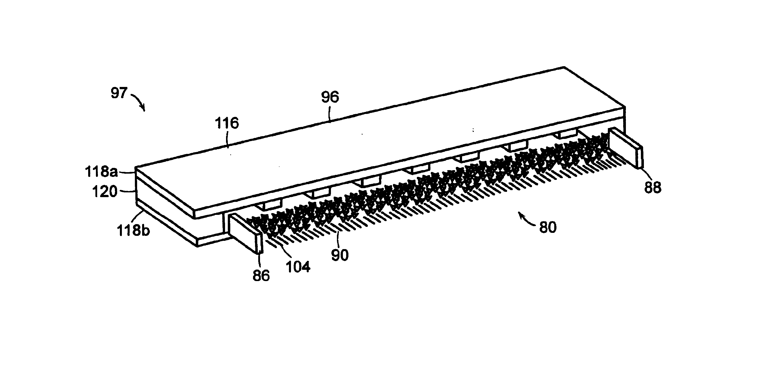
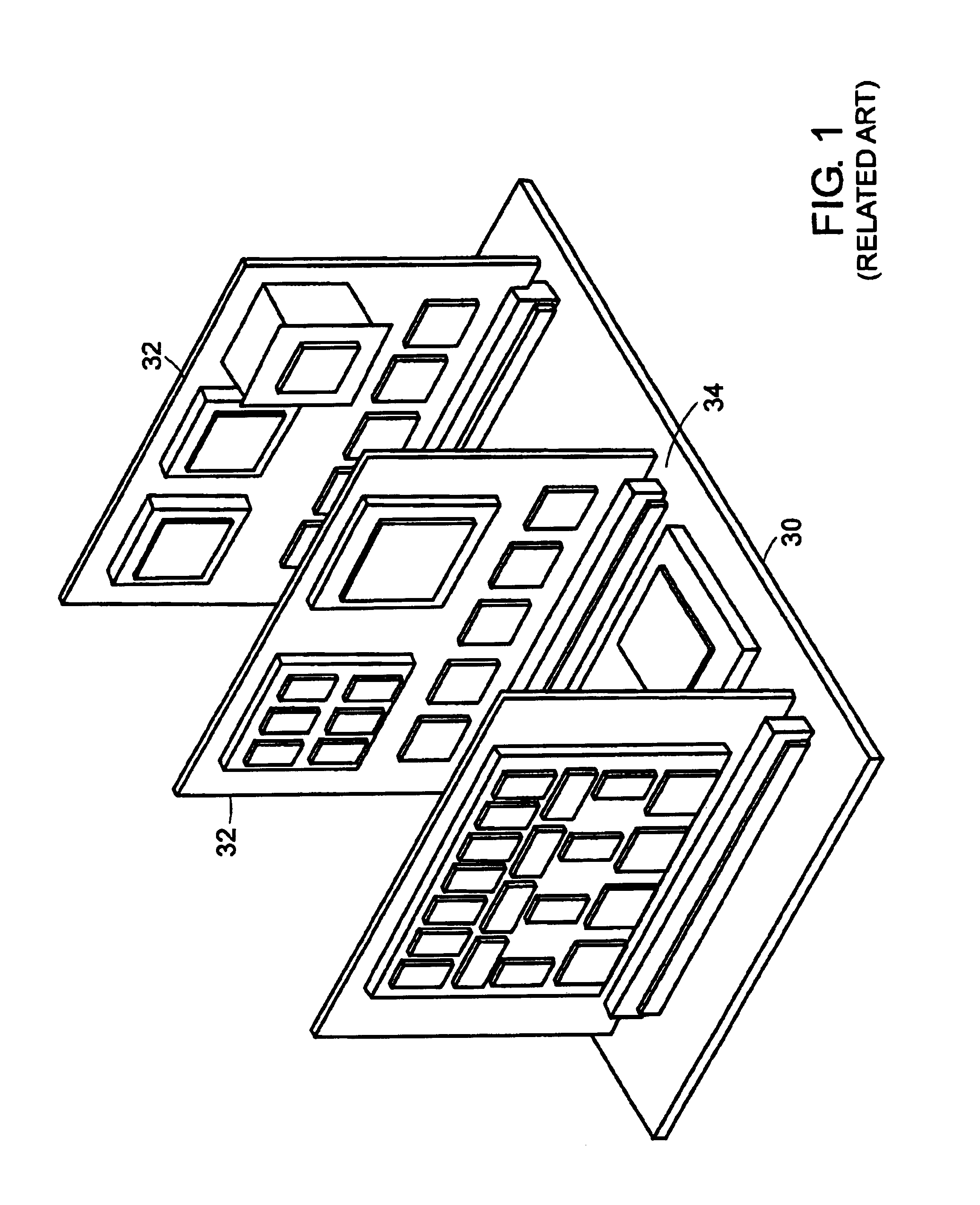
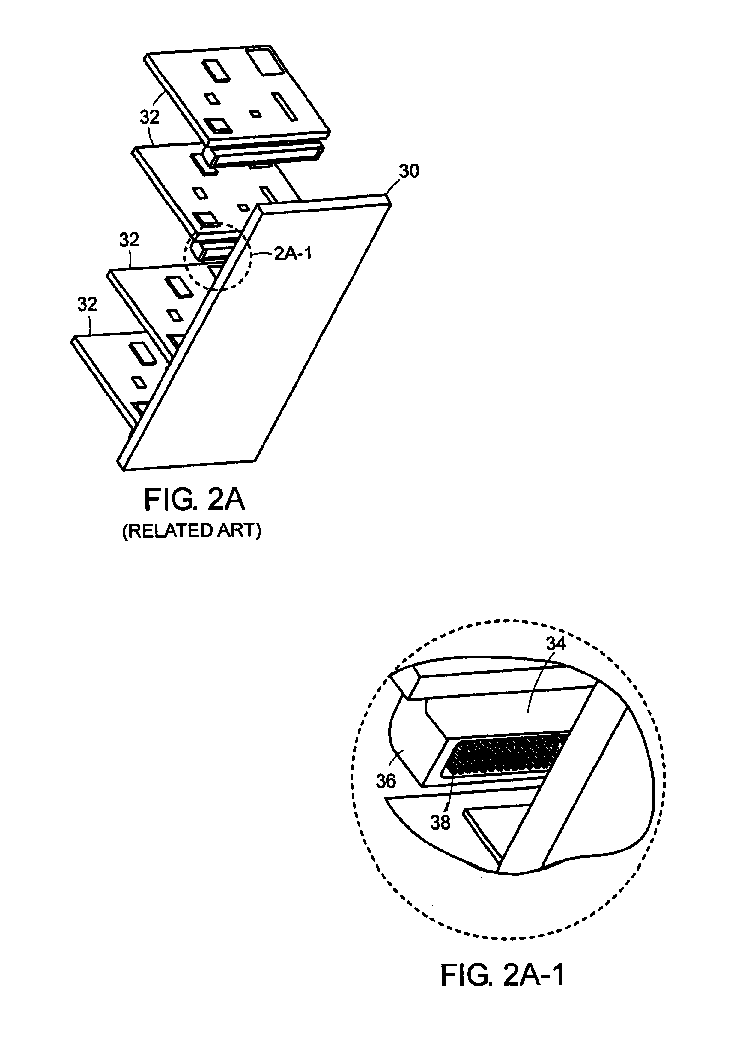
[0077]The present invention provides an electrical connector that may overcome the disadvantages of prior art connectors. The invention comprises an electrical connector capable of very high density and using only a relatively low normal force to engage a connector element with a mating connector element. It is to be understood that the invention is not limited in its application to the details of construction and the arrangement of components set forth in the following description or illustrated in the drawings. Other embodiments and manners of carrying out the invention are possible. Also, it is to be understood that the phraseology and terminology used herein is for the purpose of description and should not be regarded as limiting. The use of “including,”“comprising,” or “having” and variations thereof is meant to encompass the items listed thereafter and equivalents thereof as well as additional items. In addition, it is to be appreciated that the term “connector” as used herein...


PUM


Abstract

The present disclosure is directed to methods and devices that use a contact interface for establishing an electrical connection with an electrical component. In certain exemplary embodiments, the contact interface of a device includes at least one loading fiber and at least one conductor having at least one contact point. The conductor(s) is coupled to a loading fiber so that an electrical connection can be established between the contact point(s) of the conductor(s) and the electrical component when the device is engaged with the electrical component. In certain exemplary embodiments, a conductor is woven with, or wound around, a loading fiber. In some exemplary embodiments, the conductor is comprised of a shaped contact and a conductive lead.The present disclosure is also directed to methods and devices for testing the electrical integrity or functionality of an electrical component. In certain exemplary embodiments, the device includes a plurality of loading fibers, a plurality of conductors and a plurality of tensioning guides. Each conductor can be coupled to at least one loading fiber. The tensioning guides can be disposed on at least one side of each said conductor. In such embodiments, electrical connections can be established between at least a portion of the plurality of conductors and the electrical component when the device is engaged with the electrical component. At least a portion of the plurality of loading fibers may come into contact with the plurality of tensioning guides when the device is engaged with the electrical component. In one exemplary embodiment, the device comprises a burn-in socket device. In another exemplary embodiment, the device comprises a test socket device.

Description

FIELD OF THE INVENTION[0001]The present disclosure is directed to systems and methods for connecting one electrical component to another electrical component, and in particular to systems and methods having contact interfaces which utilize tensioned loading fibers.DISCUSSION OF RELATED ART[0002]Components of electrical systems sometimes need to be interconnected using electrical connectors to provide an overall, functioning system. These components may vary in size and complexity, depending on the type of system. For example, referring to FIG. 1, a system may include a backplane assembly comprising a backplane or motherboard 30 and a plurality of daughter boards 32 that may be interconnected using a connector 34, which may include an array of many individual pin connections for different traces etc., on the boards. For example, in telecommunications applications where the connector connects a daughter board to a backplane, each connector may include as many as 2000 pins or more. Alt...

Claims


Application Information

Patent Timeline
Patent Type & Authority Patents(United States)
IPC IPC(8): H01R12/24H01R4/58H01R13/193H05K3/10
CPCH01R4/58H05K3/10H01R13/193H05K2201/029H05K2201/0281G01R1/0416G01R1/07307H05K7/06
Inventor SWEETLAND, MATTHEW
Owner METHODE ELETRONICS INC
Why Eureka
Try Eureka