
Deposition process for high aspect ratio trenches

a high aspect ratio, trench technology, applied in the direction of chemical vapor deposition coating, coating, plasma technique, etc., can solve the problems of affecting device operation, unable to completely fill the gap of hdp-cvd films, and practical limit the aspect ratio of gaps the hdp-cvd films are able to fill

Inactive Publication Date: 2006-08-29
APPLIED MATERIALS INC
View PDF52 Cites 49 Cited by
  • Summary
  • Abstract
  • Description
  • Claims
  • Application Information

AI Technical Summary

Benefits of technology

[0009]Embodiments of the present invention deposit an insulating material that can be used to fill narrow, high aspect ratio gaps formed between adjacent raised features. Embodiments of the invention employ a multi-step sequence in which a combination of a high density plasma CVD (HDP-CVD) and atomic layer deposition (ALD) techniques are used to form the gapfill insulating material. The techniques of the invention are useful for a variety of applications including, among others, the formation of premetal dielectric layers, intermetal dielectric layers and shallow trench isolation structures in integrated circuits.
[0010]According to one embodiment of the invention, a method for depositing an insulating material having multiple layers over a substrate having a gap formed between two adjacent raised features is disclosed. The method includes depositing one layer of the insulating material over the substrate and in the gap using a high density plasma process that has simultaneous deposition and sputtering components and depositing another layer of the insulating material over the substrate and in the gap using an atomic layer deposition process. In some embodiments the layer of the material deposited by an atomic layer deposition process is deposited over the layer of the material deposited using a high density plasma CVD technique. In other embodiments, the layer of material deposited by a high density plasma CVD process is deposited over the layer of material deposited using an atomic layer deposition process. In still other embodiments a third layer of insulating material is deposited over the high density plasma and atomic layer deposition layers.
[0011]According to another embodiment, a method of depositing an insulating film over a substrate having a gap formed between two adjacent raised features includes depositing a first portion of the insulating film over the substrate and into the gap using a high density plasma process that has simultaneous deposition and sputtering components. After completion of the high density plasma process, a second portion of the insulating film is deposited over the first portion and into the gap using an atomic layer deposition process. The atomic layer deposition process includes: (i) exposing the substrate to a first reactant introduced into a chamber in which the substrate is disposed such that one or more layers of the first reactant are adsorbed onto the substrate, (ii) evacuating or purging the chamber of the first reactant, (iii) exposing the substrate to a second reactant of dissociated radicals to convert the first reactant into a thin film insulating compound and (iv) repeating the exposing, evacuating / purging and exposing sequence multiple times. Next, a third portion of the insulating film is deposited over the second portion using another high density plasma process that has simultaneous deposition and sputtering components.
[0012]These and other embodiments of the invention along with many of its advantages and features are described in more detail in conjunction with the text below and attached figures.

Problems solved by technology

Gaps having a combination of a high aspect ratio and a small width present a challenge for semiconductor manufacturers to fill completely.
In short, the challenge usually is to prevent the film from forming in a manner that closes off the gap before it is filled.
Failure to fill a gap completely results in the formation of a void in the deposited layer, which may adversely affect device operation.
Thus, the filling of trenches 24 is typically one of the most challenging gapfill applications in the formation of the integrated circuit.
Semiconductor manufacturers have found out, however, that there is a practical limit to the aspect ratio of gaps that HDP-CVD films are able to fill.

Method used


Image

  • Deposition process for high aspect ratio trenches
  • Deposition process for high aspect ratio trenches
  • Deposition process for high aspect ratio trenches

Examples


Embodiment Construction

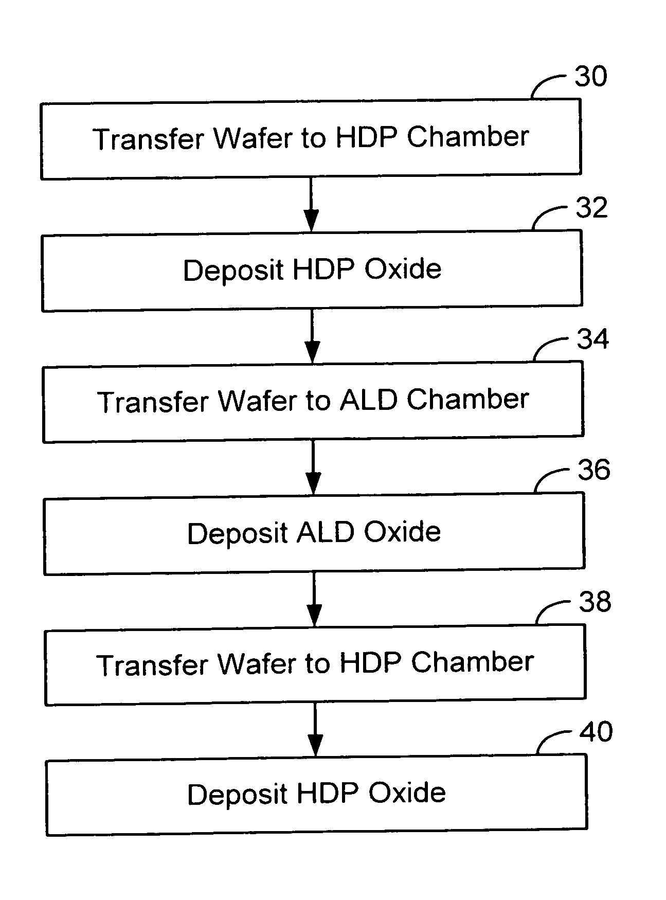
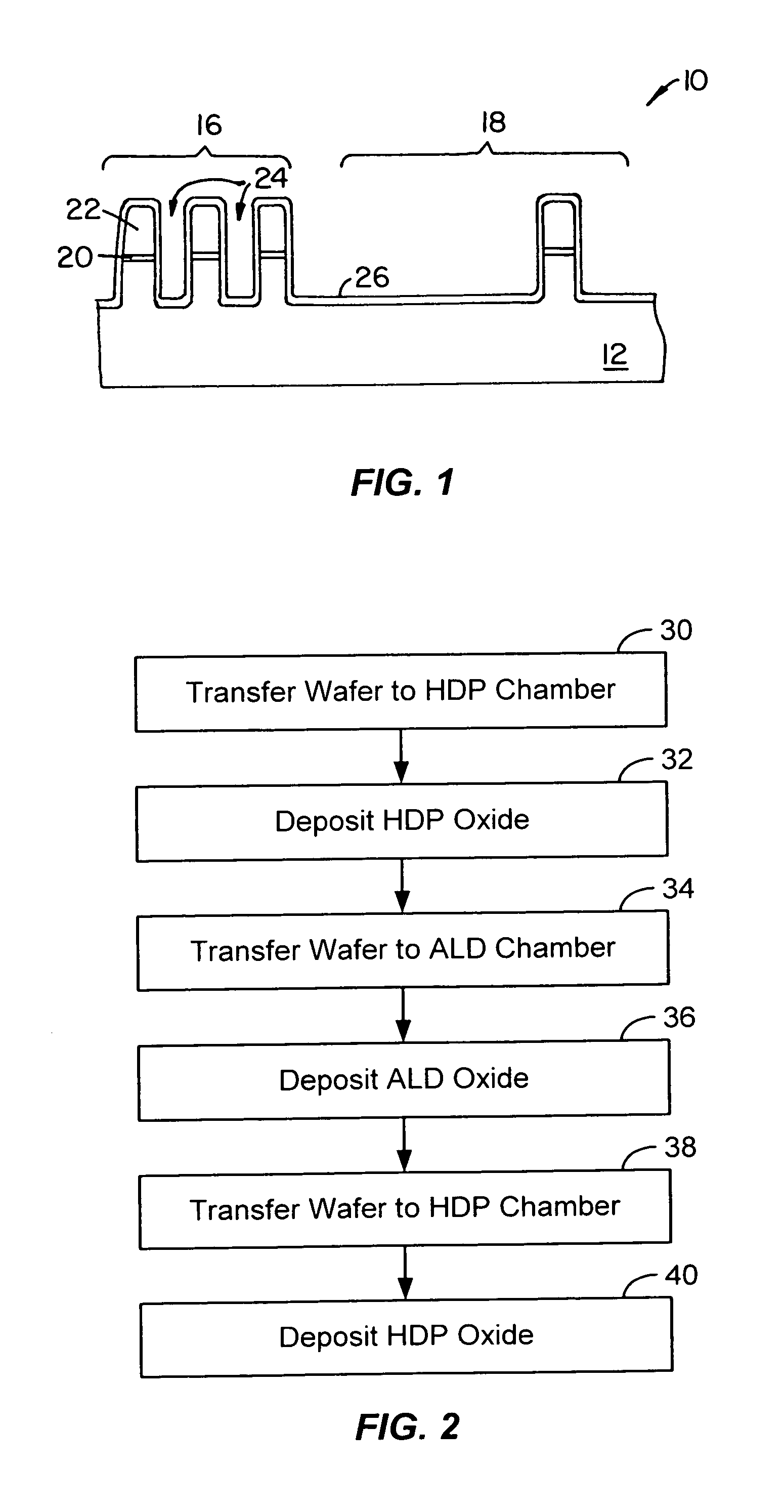
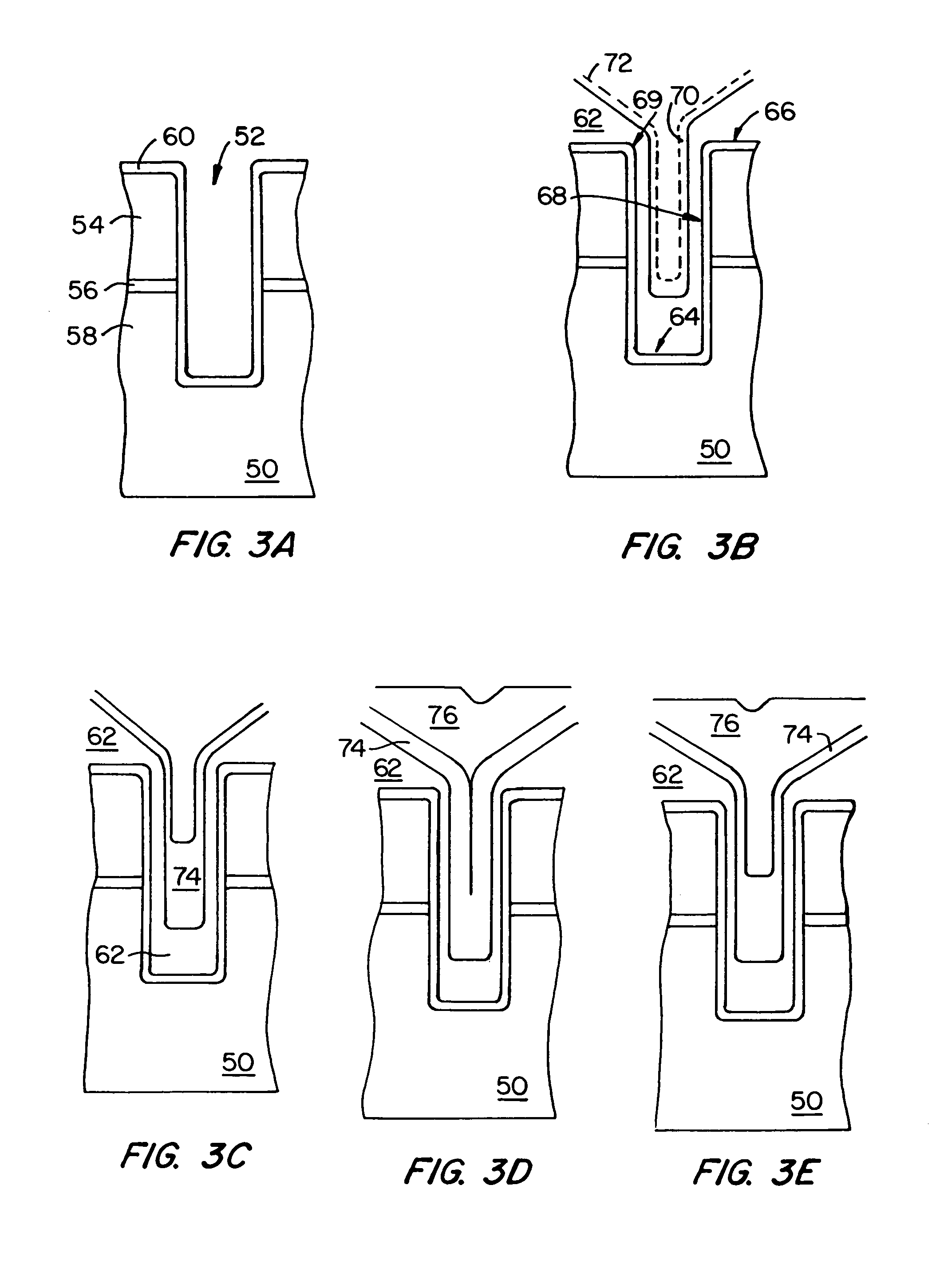
[0020]Embodiments of the invention pertain to a multi-step process for depositing a multilayer dielectric material into high aspect ratio features. Embodiments of the invention permit the dielectric material to be deposited with substantially 100% gapfill for most currently envisioned small-width, high aspect ratio applications. For example, for gaps having a width of 0.10 microns substantially 100% gapfill can be achieved by embodiments of the invention for aspect ratios of 8:1 and even higher in both the active and open areas of an integrated circuit die. Embodiments of the invention are useful for a variety of different applications and are particularly useful for the fabrication of integrated circuits having minimum feature sizes of 0.10 microns or less.

[0021]Embodiments of the invention employ a combination of high density plasma CVD (HDP-CVD) and atomic layer deposition (ALD) techniques to deposit the insulating film within the gaps to be filled. In some embodiments, a first l...


PUM

PropertyMeasurementUnit
aspect ratioaaaaaaaaaa
widthaaaaaaaaaa

Abstract

A method of depositing an insulating film over a substrate having a gap formed between two adjacent raised features. The method includes depositing one portion of the insulating film over the substrate and in the gap using a high density plasma process that has simultaneous deposition and sputtering components and depositing another portion of the insulating film over the substrate and in the gap using an atomic layer deposition process. In some embodiments the portion of the film deposited by an atomic layer deposition process is deposited over the portion of the film deposited using a high density plasma CVD technique. In other embodiments, the portion of the film deposited by a high density plasma CVD process is deposited over the portion of the film deposited using an atomic layer deposition process.

Description

BACKGROUND OF THE INVENTION[0001]One of the primary steps in the fabrication of modern semiconductor devices is the formation of an insulation film on a semiconductor substrate. Such insulation films are used for a variety of purposes including, among others, separating adjacent conductive layers (e.g., an intermetal dielectric (IMD) layer separates adjacent metal lines while a premetal dielectric (PMD) layer separates metal layer one from the conductive substrate) and separating adjacent active regions of the substrate (e.g., as part of a shallow trench isolation (STI) structure).[0002]For applications such as the deposition of IMD or PMD layers in an integrated circuit or the formation of STI structures, one important physical property of the insulation film is its ability to completely fill gaps between adjacent structures without leaving voids within the gap. This property is referred to as the film's gapfill capability. Gaps that may require filling include spaces between adjac...

Claims


Application Information

Patent Timeline
Patent Type & Authority Patents(United States)
IPC IPC(8): H05H1/24C23C16/04H01L21/316H01L21/762
CPCC23C16/045H01J37/32082H01L21/02164H01L21/76229H01L21/02274H01L21/0228H01L21/31612H01L21/022H01J2237/3327
Inventor MOGHADAM, FARHAD K.COX, MICHAEL S.KRISHNARAJ, PADMANABHANPHAM, THANH N.CUI, ZHENJIANG
Owner APPLIED MATERIALS INC
Features
  • Generate Ideas
  • Intellectual Property
  • Life Sciences
  • Materials
  • Tech Scout
  • Unparalleled Data Quality
  • Higher Quality Content
  • 60% Fewer Hallucinations
Learn More