Method and apparatus for machining substrate

Inactive Publication Date: 2006-08-29
TOKYO SEIMITSU
View PDF16 Cites 2 Cited by
  • Summary
  • Abstract
  • Description
  • Claims
  • Application Information

AI Technical Summary

Benefits of technology

[0009]Namely, according to the first embodiment, the strength of the cut surface is increased because chippings which may be formed in the cut surface are melted to form

Problems solved by technology

However, in the substrate machining method disclosed in Japanese Unexamined Patent Publication (Kokai) No. 2002-75919, there is a possibility that some problem may occur on a cut surface of the wafer. FIG. 4 is an enlarged sectional view of a diced substrate in a prior art. FIG. 5 is a partial pe

Method used


Image

  • Method and apparatus for machining substrate
  • Method and apparatus for machining substrate
  • Method and apparatus for machining substrate

Examples


Embodiment Construction

[0017]Embodiments of the present invention will be described below with reference to the accompanying drawings. In the drawings, the same members are designated by the same reference numerals. For easy understanding, the scale of each drawing is appropriately changed.

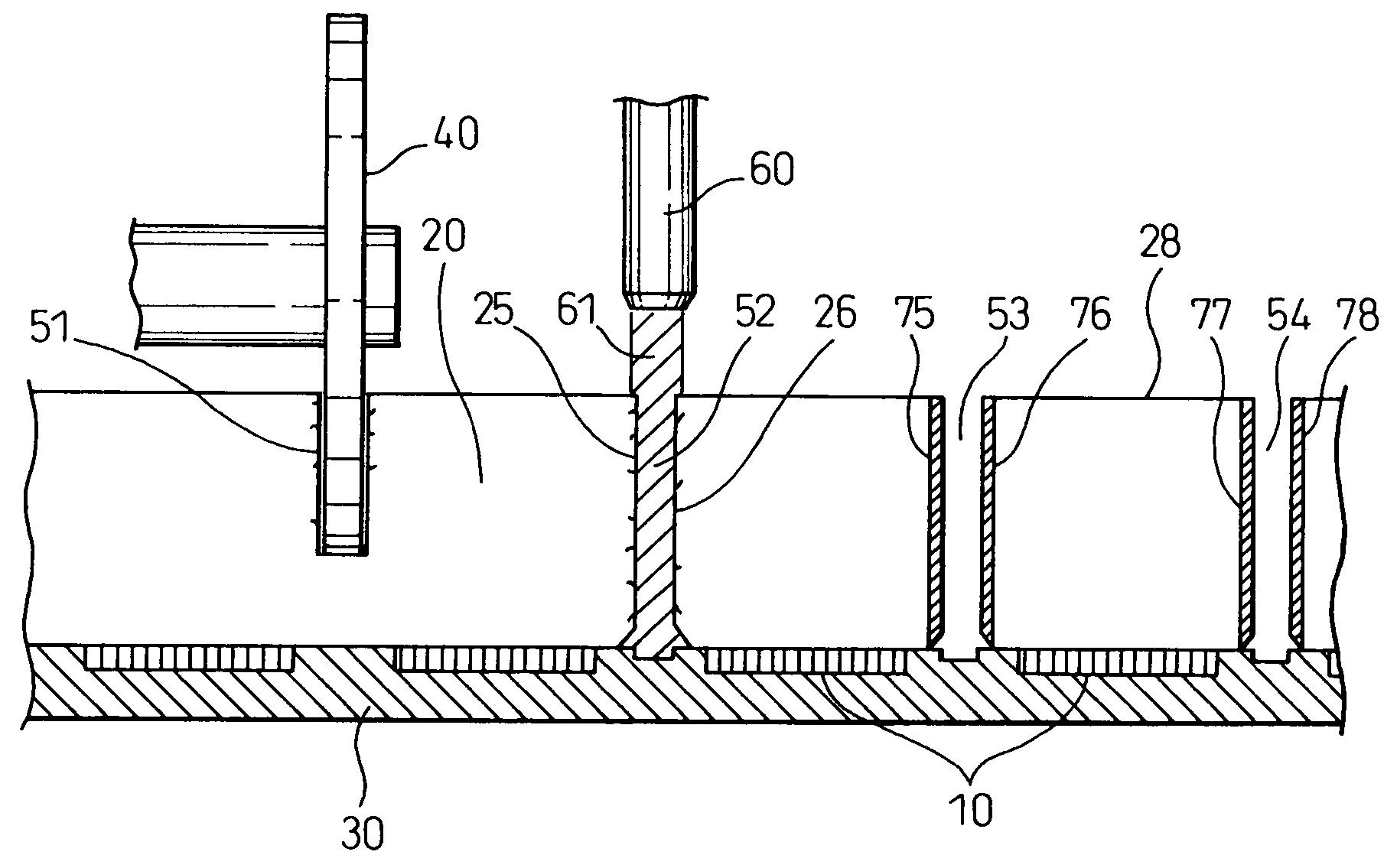
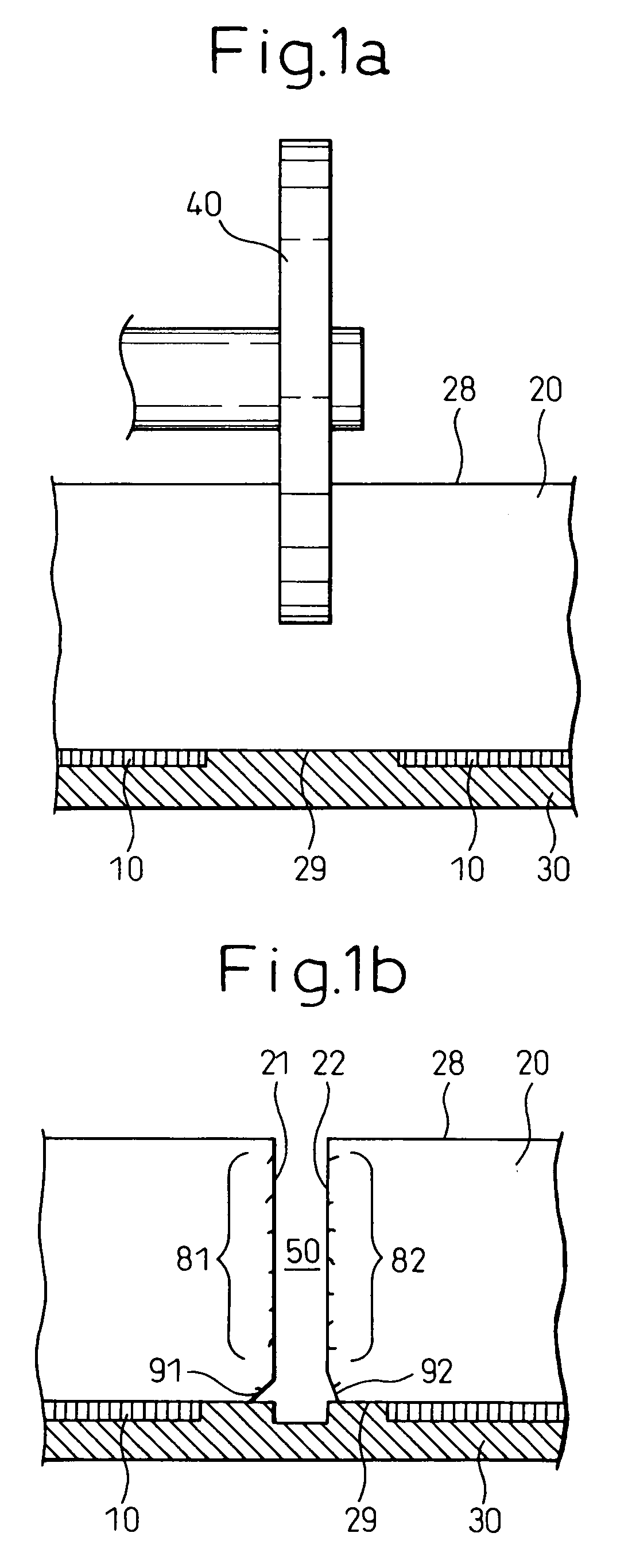
[0018]FIGS. 1a and 1b are conceptual views showing a cutting operation of a substrate machining method according to the present invention. As shown in FIG. 1a, semiconductor elements 10 are formed on a semiconductor substrate and, for example, on a silicon wafer 20. Usually, semiconductor elements 10 are formed in the shape of dice on the wafer 20. However, for easy understanding, only two semiconductor elements are shown in FIGS. 1 and 2. As can be seen from FIGS. 1a and 1b, a patterned surface 29 of the wafer 20, on which semiconductor elements 10 are formed, is covered with a dicing tape 30 or a protective film 30.

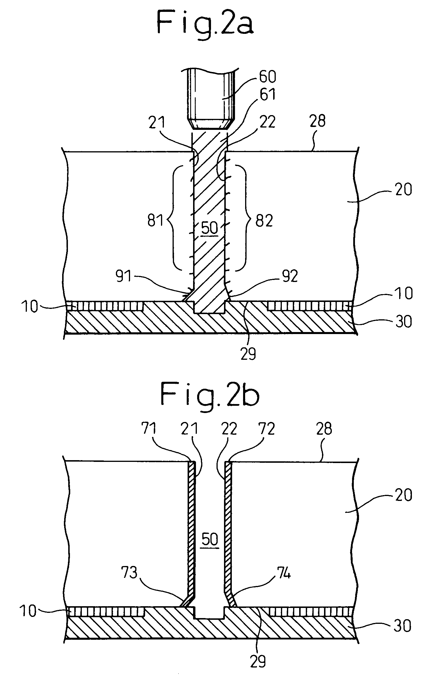
[0019]The substrate machining apparatus according to the present invention contains a disk-like blade 40...


PUM


Abstract

In a substrate machining method for machining a substrate, there are provided a substrate machining method in which a disk-like blade is rotated to cut the substrate from its one surface, and the cut surfaces of the substrate, which are positioned in the vicinity of the other surface of the substrate, are irradiated with laser light; and a substrate machining apparatus which carries out the substrate machining method. The entirety of the cut surfaces of the substrate may be irradiated with the laser light. The laser may be a YAG laser or a CO2 laser. Further, a dicing tape may be adhered to the other surface of the substrate, and the laser light may be irradiated after cutting only the substrate and expanding the dicing tape. Modified layers are formed by an irradiation of the laser light, so that dice are prevented from being broken in an assembling operation of the dice.

Description

CROSS-REFERENCE TO RELATED APPLICATION[0001]This application claims priority of Japanese Patent Application Number 2002-381129, filed on Dec. 27, 2002.BACKGROUND OF THE INVENTION[0002]1. Field of the Invention[0003]The present invention relates to a method and apparatus for machining a substrate such as, for example, a semiconductor wafer.[0004]2. Description of the Related Art[0005]In the field of manufacturing semiconductors, the dicing process for cutting a substrate such as, for example, a silicon wafer on which a plurality of semiconductor elements are formed, into cubic portions, i.e., dicing a substrate, is necessary. A substrate machining apparatus for dicing contains a disk-like blade. Before a dicing process, an adhesive dicing tape is attached to a wafer. After that, the blade is rotated to cut the wafer from its surface, on which no dicing tape is attached, while cutting water is supplied to the wafer. The blade is moved forward to form a street. Usually, only the wafer ...

Claims


Application Information

Patent Timeline
IPC IPC(8): H01L21/46H01L21/301H01L21/78B23K26/38B23K26/40B23K101/40B28D1/22B28D5/02
CPCB28D5/022B28D1/221B23K2201/40B23K2101/40H01L21/78
Inventor KOBAYASHI, KAZUO
Owner TOKYO SEIMITSU
Why Eureka
Try Eureka