Method and apparatus for resetting a high speed latch circuit

a high-speed latch and circuit technology, applied in pulse technique, optical radiation measurement, instruments, etc., can solve the problems of not being satisfactory in all respects, affecting the normal electrical balance of the latch, and effectively introducing the dynamic gate current of the

Active Publication Date: 2006-08-29
RAYTHEON CO
View PDF4 Cites 23 Cited by
  • Summary
  • Abstract
  • Description
  • Claims
  • Application Information

AI Technical Summary

Benefits of technology

[0007]From the foregoing, it may be appreciated that a need has arisen for a method and apparatus for resetting a high-speed latch circuit, in a manner which avoids at least the known problem of clock injection. According to the present invention, a method and apparatus are provided to address this need, in a context where a latch circuit has first and second resonant tunneling diodes coupled in series with each other between first and second nodes, and a reset portion coupled to the first and second nodes. The method and apparatus involve: configuring the reset portion to include a photodiode portion which is responsive to varying photonic energy for switching between first and second states that are different; and causing the photodiode portion to normalize a voltage across each of the resonant tunneling diodes when the reset portion is in its first state.

Problems solved by technology

Although this configuration has been generally adequate for its intended purpose, it has not been satisfactory in all respects.
For example, one disadvantage is that the dynamic gate current of the FET is effectively introduced into the operation of the latch circuit, which is a phenomenon commonly known as “clock injection”.
This current passes through the drain and source nodes of the FET and into the RTD circuitry, and can upset the normal electrical balance of the latch, which in turn prevents the latch from accurately capturing the value of the data input signal.
This disadvantageous effect of clock injection increases with the frequency of the clock, so that the known latch circuit is limited in its frequency of operation by the effect of clock injection.

Method used


Image

  • Method and apparatus for resetting a high speed latch circuit
  • Method and apparatus for resetting a high speed latch circuit
  • Method and apparatus for resetting a high speed latch circuit

Examples


Embodiment Construction

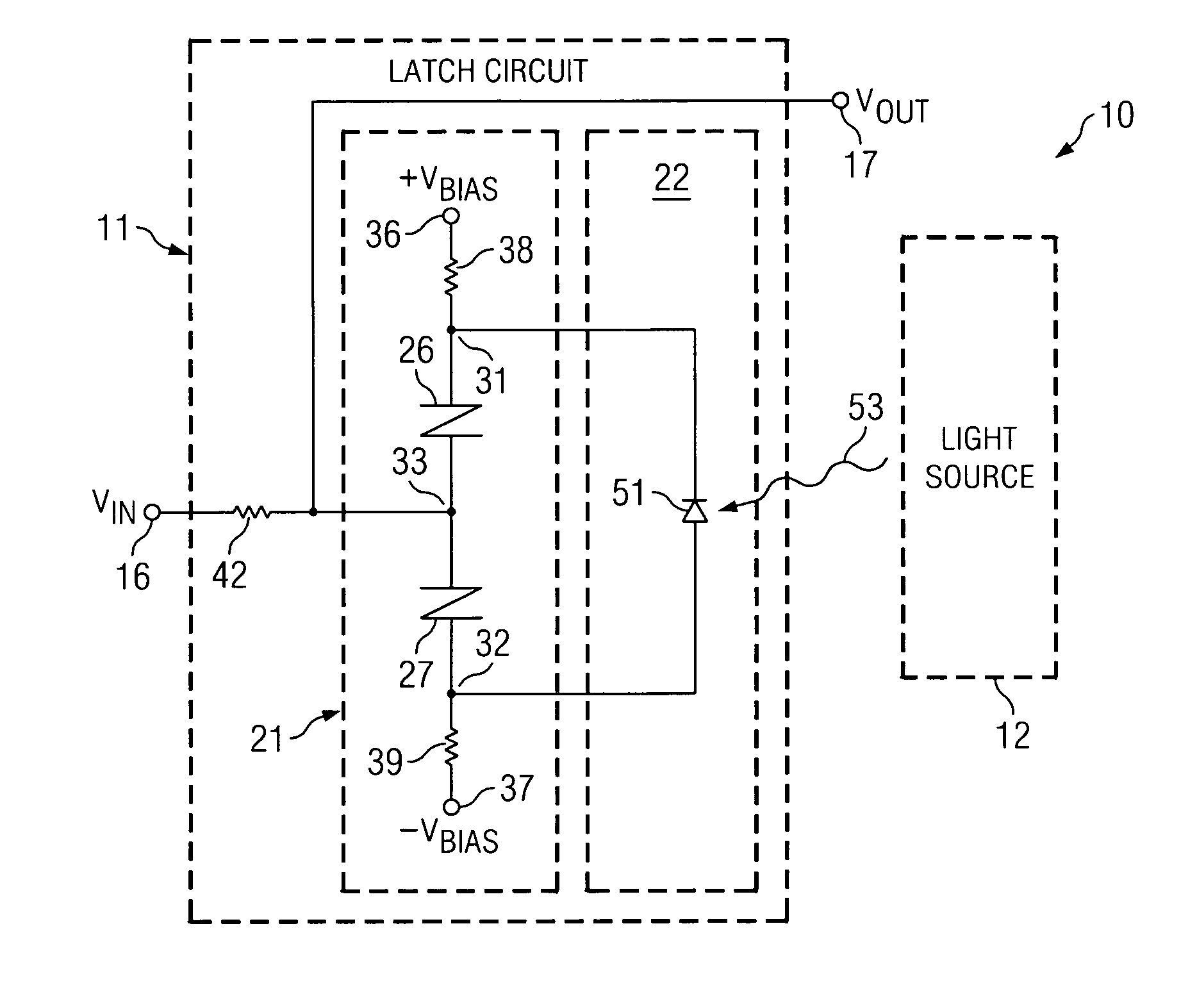
[0015]FIG. 1 is a schematic diagram of an apparatus 10 which includes a latch circuit 11 and a light source 12. The latch circuit 11 has an input terminal 16, to which an input voltage VIN is applied, and has an output terminal 17, at which the latch circuit 11 produces an output voltage VOUT.

[0016]The latch circuit 11 includes a latch portion 21, and a recess portion 22. The latch portion 21 includes two resonant tunneling diodes (RTDs) 26 and 27 of a known type, which are coupled in series between two nodes 31 and 32, with a further node 33 defined between the RTDs 26 and 27. The latch portion 21 has a bias terminal 36, to which is applied a positive direct current (DC) bias voltage +VBIAS. The latch portion 21 has a further bias terminal 37, to which is applied a negative DC bias voltage −VBIAS. The bias voltages applied to the bias terminals 36 and 37 are opposite in polarity, but equal in magnitude.

[0017]The latch portion 21 includes a resistor 38 which is coupled between the b...


PUM


Abstract

A latch circuit includes first and second resonant tunneling diodes coupled in series, and a reset portion having a photodiode portion responsive to varying photonic energy for switching between first and second states which are different. When the photodiode portion is in its first state, the reset portion normalizes a voltage across each of the resonant tunneling diodes.

Description

GOVERNMENT INTEREST[0001]This invention was made with Government support under Contract No. N00014-98-3-0013. The Government has certain rights in this invention.TECHNICAL FIELD OF THE INVENTION[0002]This invention relates in general to high-speed latch circuits and, more particularly, to techniques for resetting a high-speed latch circuit.BACKGROUND OF THE INVENTION[0003]High-speed latches can be used to build sophisticated digital processing systems, such as those used to process microwave signals. These latches store digital data under the action of a clock signal. Where the clock signal has a high frequency, for example above 1 GHz and up to 500 GHz or more, one known type of latch has two resonant tunneling diodes (RTDs), which are coupled in series and which operate at GHz clock rates with very low power consumption.[0004]In these known latch circuits, the series-coupled RTDs receive electrical power from a current-limited voltage source, which may for example be a battery and...

Claims


Application Information

Patent Timeline
Patent Type & Authority Patents(United States)
IPC IPC(8): H03F3/08G01J5/00H03K17/78
CPCH03K3/315
Inventor FRAZIER, GARY A.
Owner RAYTHEON CO
Why Eureka
Try Eureka