Single cycle read/write/writeback pipeline, full-wordline I/O DRAM architecture with enhanced write and single ended sensing

a dram architecture and read/write/writeback pipeline technology, applied in the field of dram memories, can solve problems such as not being able to meet the state of the art in speed and bandwidth, and achieve the effect of increasing the overall i/o width and increasing the number of banks

Inactive Publication Date: 2006-08-29
GLOBALFOUNDRIES INC
View PDF9 Cites 56 Cited by
  • Summary
  • Abstract
  • Description
  • Claims
  • Application Information

AI Technical Summary

Benefits of technology

[0006]It is a further object to teach this DRAM architecture incorporating a full-wordline I / O structure for Read / Write / WriteBack with small global bitline signal swing, resulting in low active power and low noise coupling during Read / Write operation.
[0010]It is a further object in exemplary embodiments the invention to teach a new, area efficient PSA which comprise at least two amplification stages, high gain, single ended sensing buffers, feedback circuit for enhanced WriteBack / Write operations and the global bitline isolation “cut-off” device. The Read / Write / WriteBack operations and their controls can be combined area-efficiently in a PSA circuit which can have as few as 6 FET devices. There can be one more NFET per bitline for bitline multiplexing. The two stage buffer arrangement enables the first stage to amplifier a small bitline signal (e.g. 200 mV) to almost fill Vdd swing (e.g. 1V) to drive the second stage which has enough gate overdrive to handle a long, heavily capacitance loaded global bitline. Such structure results in small sense amplifier PET devices that can drive a long global bitline (GBL) spanning a typical chip (e.g. 10 mm).
[0013]A further embodiment of the present invention teaches a two dimensional growable structure by combining macros to form a bigger DRAM, or EDRAM, with shared input, output, command and address buses running in orthogonal direction to the macros. The command, address and data can be distributed to the macros, and data returned to the overall I / O with minimum skew. The floorplan is growable in two dimensions, vertically within a macro in term of the number of arrays, and horizontally in terms of the number of macros. The overall structure can be used to increase overall I / O width and / or to increase number of banks. The overall structure can perform simultaneous Read / Write in the same cycle at different banks located in non-overlapping macros. WriteBack and Read / Write can be performed in the same macro within the same cycle.

Problems solved by technology

DRAM memories traditionally lead in storage density but typically they are not the state of the art in speed and bandwidth.

Method used


Image

  • Single cycle read/write/writeback pipeline, full-wordline I/O DRAM architecture with enhanced write and single ended sensing
  • Single cycle read/write/writeback pipeline, full-wordline I/O DRAM architecture with enhanced write and single ended sensing
  • Single cycle read/write/writeback pipeline, full-wordline I/O DRAM architecture with enhanced write and single ended sensing

Examples


Embodiment Construction

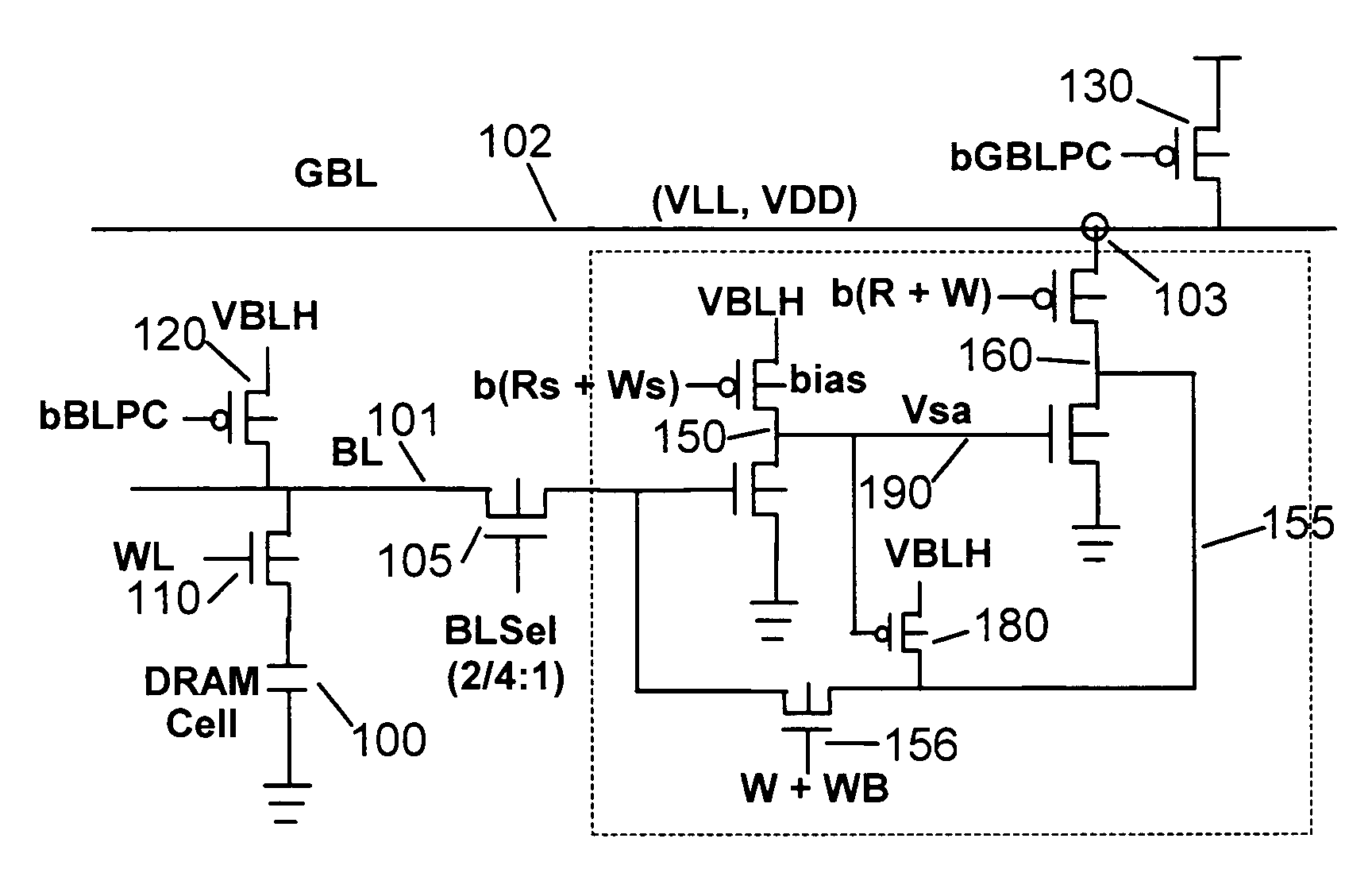
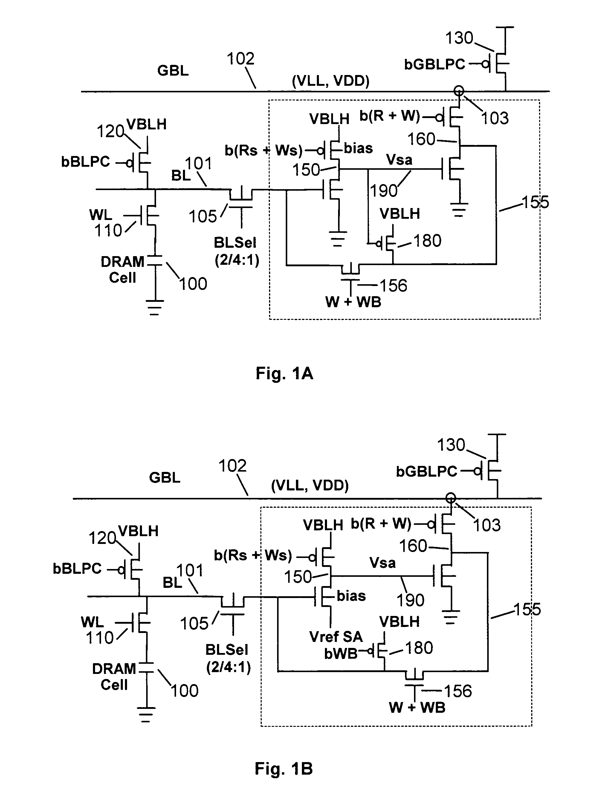
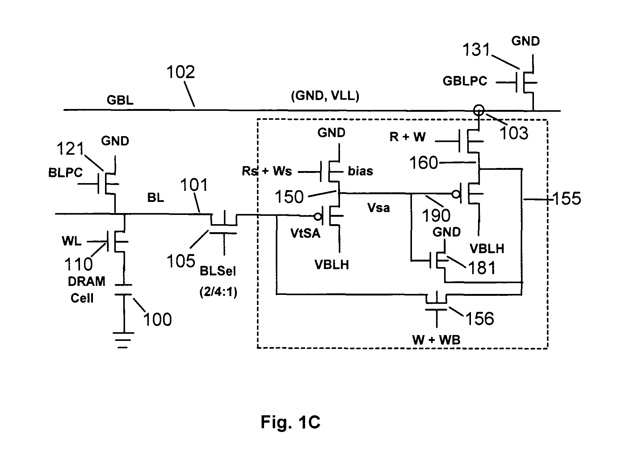
[0029]FIG. 1 shows exemplary embodiments of DRAM primary sense amplifiers with data storage and data write-back capability, and two amplification stages. The DRAM memory cell capacitor 100 is connected to a single ended bitline 101 under the control of the wordline (WL) 110 of the transfer device. The single ended bitline 101 exemplifies the embodiment of a single ended bitline structure, where the storage cell connects to the primary sense amplifier (PSA) by only one single bitline. In FIG. 1 the PSA is made up the circuits enclosed in the dashed rectangle. The bitline 101 access to the PSA is controlled by a multiplexer device 105. In an exemplary embodiment the PSA-s are located between two adjacent DRAM arrays, and each PSA is shared between four bitlines by using multiplexers 105. The four bitlines are: two bitlines (odd and even) from the upper array and two bitlines (odd and even) from the lower array, since one array (bank) is active, and only either an odd or an even bitlin...


PUM


Abstract

A DRAM is disclosed which includes a single ended bitline structure, a single ended global bitline structure, primary sense amplifiers with data storage and data write-back capability and with capability to decouple from the global bitlines, a full-wordline I / O structure where essentially all memory cell that belong to the same wordline are being operated on, and a pipelined architecture. The DRAM further includes a small voltage swing design. The primary sense amplifiers can include more than one amplification stages. Such a DRAM is suitable for applications in conjunction with processors as an embedded DRAM.

Description

FIELD OF THE INVENTION[0001]The present invention relates to DRAM memories that have high data throughput rates and speed. In particular, exemplary embodiments of this invention deal with embedded DRAM macros of novel architecture.BACKGROUND OF THE INVENTION[0002]Today's integrated circuits include a vast number of transistor devices formed in a semiconductor. Smaller devices are the key to enhance performance and to increase reliability. As devices are scaled down, however, the technology becomes more complex and new methods are needed to maintain the expected performance enhancement from one generation of devices to the next. The storage capacity, speed, and data throughput rates of memories has to keep up with processor improvements.SUMMARY OF THE INVENTION[0003]DRAM memories traditionally lead in storage density but typically they are not the state of the art in speed and bandwidth. Modern high performance processors need both a large amount of data and rapid access to it. The l...

Claims


Application Information

Patent Timeline
Patent Type & Authority Patents(United States)
IPC IPC(8): G11C7/00G11C7/06G11C7/10G11C11/24G11C11/4091
CPCG11C7/067G11C11/4091G11C7/1039G11C2207/104
Inventor LUK, WING K.DENNARD, ROBERT H.
Owner GLOBALFOUNDRIES INC
Why Eureka
Try Eureka