Active matrix substrate and display device

a technology of active matrix substrate and display device, which is applied in the direction of semiconductor devices, instruments, optics, etc., can solve the problems of difficult formation of demux circuits using oxide semiconductor tft, and achieve the effect of reducing the driving power of active matrix substrates provided with demultiplexer circuits

Active Publication Date: 2020-12-31
SHARP KK
View PDF0 Cites 1 Cited by
  • Summary
  • Abstract
  • Description
  • Claims
  • Application Information

AI Technical Summary

Benefits of technology

[0010]Because the mobility of an oxide semiconductor is approximately an order of magnitude smaller than polycrystalline silicon, an oxide semiconductor TFT has a smaller current driving force than a polycrystalline silicon TFT. For this reason, in the case of using an oxide semiconductor to form the DEMUX circuit TFT, it is necessary to increase the size of the TFT (increase the channel width) or raise the driving voltage compared to the case of using polycrystalline silicon. If the size of the TFT is increased, the gate capacitance load increases, and the driving power of the DEMUX circuit increases. On the other hand, raising the driving voltage of the TFT also increases the driving power of the DEMUX circuit.
[0099]According to an embodiment of the present invention, the driving power of an active matrix substrate provided with a demultiplexer circuit can be reduced.

Problems solved by technology

However, it is difficult to form the DEMUX circuit using an oxide semiconductor TFT, and in the past, a polycrystalline silicon TFT has been used as the DEMUX circuit TFT.
Note that, as described later, even in the case of using a polycrystalline silicon TFT as the DEMUX circuit TFT, a similar problem may occur if only PMOS processes are adopted (that is, if the polycrystalline silicon TFT contains PMOS transistors only).

Method used


Image

  • Active matrix substrate and display device
  • Active matrix substrate and display device
  • Active matrix substrate and display device

Examples


embodiment 1

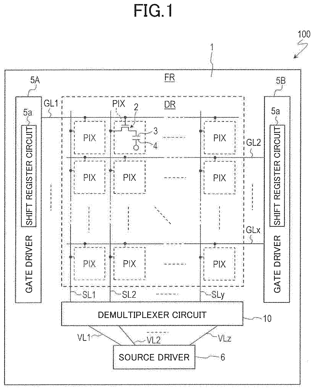
[0122]FIG. 1 is a schematic diagram illustrating one example of a plan-view structure of an active matrix substrate 100 according to the present embodiment. As illustrated in FIG. 1, the active matrix substrate 100 includes a display region DR and a peripheral region FR.

[0123]The display region DR includes a plurality of pixel regions PIX. The pixel regions PIX are regions corresponding to the pixels of the display device. Hereinafter, the pixel regions PIX will also simply be referred to as the “pixels”. The plurality of pixel regions PIX are arranged in a matrix containing a plurality of rows and a plurality of columns. The display region DR is prescribed by the plurality of pixel regions PIX arranged in a matrix.

[0124]The peripheral region FR is positioned in the periphery of the display region DR. The peripheral region FR is a region that does not contribute to display, and may also be referred to as the “non-display region” or the “bezel region”.

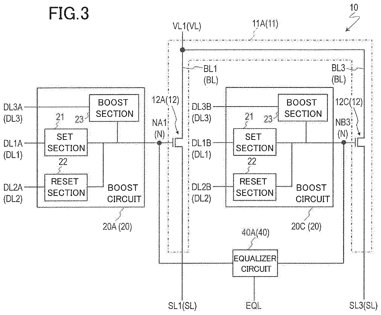
[0125]Components of the active m...

embodiment 2

[0180]An active matrix substrate according to the present embodiment will be described with reference to FIG. 7. FIG. 7 is a diagram illustrating a configuration of a DEMUX circuit 10A provided in the active matrix substrate of the present embodiment.

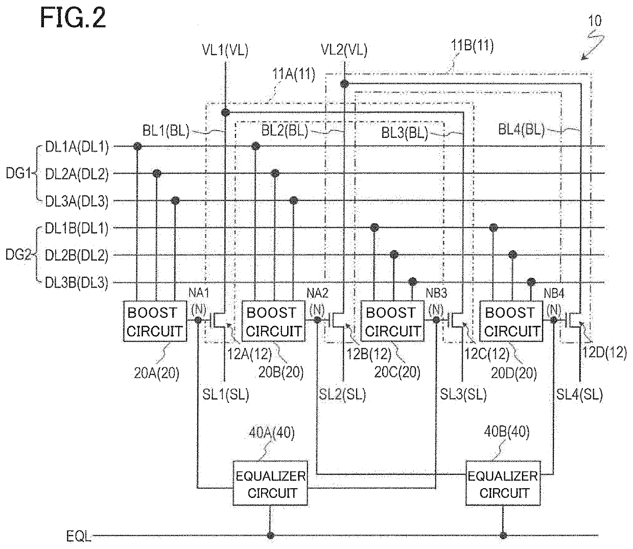
[0181]As illustrated in FIG. 7, the DEMUX circuit 10A in the present embodiment differs from the DEMUX circuit 10 illustrated in FIG. 2 by not including the second driving signal line DL2.

[0182]Here, if attention is focused on the first boost circuit 20A and the second boost circuit 20C connected to the first switching TFT 12A and the second switching TFT 12C of the first unit circuit 11A, the first boost circuit 20A is connected to a first driving signal line DL1A and a third driving signal line DL3A for the first boost circuit 20A, and is also connected to the first driving signal line DL1B for the second boost circuit 20C. Also, the second boost circuit 20C is connected to the first driving signal line DL1B and the third driving sign...

embodiment 3

[0211]An active matrix substrate according to the present embodiment will be described with reference to FIG. 11.

FIG. 11 is a diagram illustrating a configuration of a DEMUX circuit 10B provided in the active matrix substrate of the present embodiment.

[0212]In the DEMUX circuit 10 illustrated in FIG. 2, one boost circuit 20 is connected to each switching TFT 12. In contrast, in the DEMUX circuit 10B of the present embodiment, as illustrated in FIG. 11, one boost circuit 20 is connected to two switching TFTs 12. Hereinafter, a more specific description will be given.

[0213]Of the two boost circuits 20A and 20B illustrated in FIG. 11, one (first boost circuit) 20A is connected in common with the first switching TFT 12A of the first unit circuit 11A and the first switching TFT 12B of the second unit circuit 11B. Also, the other (second boost circuit) 20B is connected in common with the second switching TFT 12C of the first unit circuit 11A and the second switching TFT 12D of the second ...


PUM

PropertyMeasurementUnit
voltageaaaaaaaaaa
charge-aaaaaaaaaa
semiconductoraaaaaaaaaa

Abstract

An active matrix substrate is provided with a demultiplexer circuit. Each unit circuit of the demultiplexer circuit splits the display signal from a single signal output line to n source bus lines. Each unit circuit includes n branch lines and n switching TFTs. The demultiplexer circuit includes boost circuits configured to boost the voltage applied to the gate electrodes of the switching TFTs. Each boost circuit includes a set section that pre-charges a node connected to the gate electrode, a boost section that boosts the potential of the node pre-charged by the set section, and a reset section that resets the potential of the node. The demultiplexer circuit includes an equalizer circuit configured to perform charge sharing by electrically connecting a first node boosted by the boost section of a first boost circuit and a second node boosted by the boost section of a second boost circuit.

Description

CROSS-REFERENCE TO RELATED APPLICATION[0001]The present application claims priority from Provisional Application No. 62 / 867,929, the content to which is hereby incorporated by reference into this application.BACKGROUND OF THE INVENTION1. Field of the Invention[0002]The present invention relates to an active matrix substrate, and more particularly to an active matrix substrate provided with a demultiplexer circuit. In addition, the present invention also relates to a display device provided with such an active matrix substrate.2. Description of the Related Art[0003]An active matrix substrate used in a display device or the like includes a display region having a plurality of pixels and a region other than the display region (a non-display region or bezel region). In the display region, a switching element such as a thin-film transistor (TFT) is provided for every pixel. In the past, a TFT using amorphous silicon film as an active layer (hereinafter referred to as an amorphous silicon...

Claims


Application Information

Patent Timeline
Patent Type & Authority Applications(United States)
IPC IPC(8): G02F1/1368H01L27/12G09G3/36
CPCH01L27/1225G09G3/3648H01L27/1251G09G2310/0297G02F1/1368G02F1/13452G02F1/133G02F1/136286G02F1/1685G09G3/3225G09G3/344H01L27/124G09G2330/023G09G2310/0248G09G3/3688G09G2310/0291
Inventor YAMAMOTO, KAORU
Owner SHARP KK
Why Eureka
Try Eureka