Storage circuit, semiconductor device, and electronic apparatus
a technology of semiconductor devices and electronic devices, applied in mechanical devices, transportation and packaging, instruments, etc., can solve problems such as static cell malfunction and complex operation, and achieve the effect of suppressing the deterioration of the first ferroelectric capacitor and the second ferroelectric capacitor
- Summary
- Abstract
- Description
- Claims
- Application Information
AI Technical Summary
Benefits of technology
Problems solved by technology
Method used
Image
Examples
first embodiment
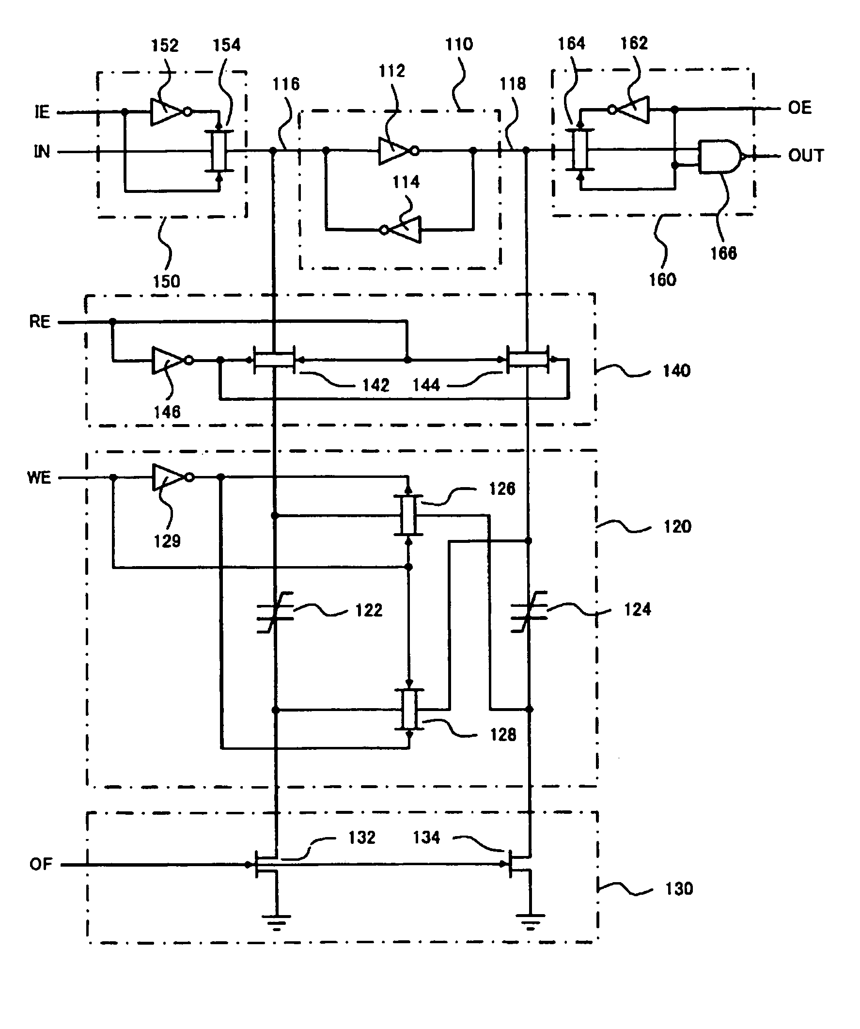
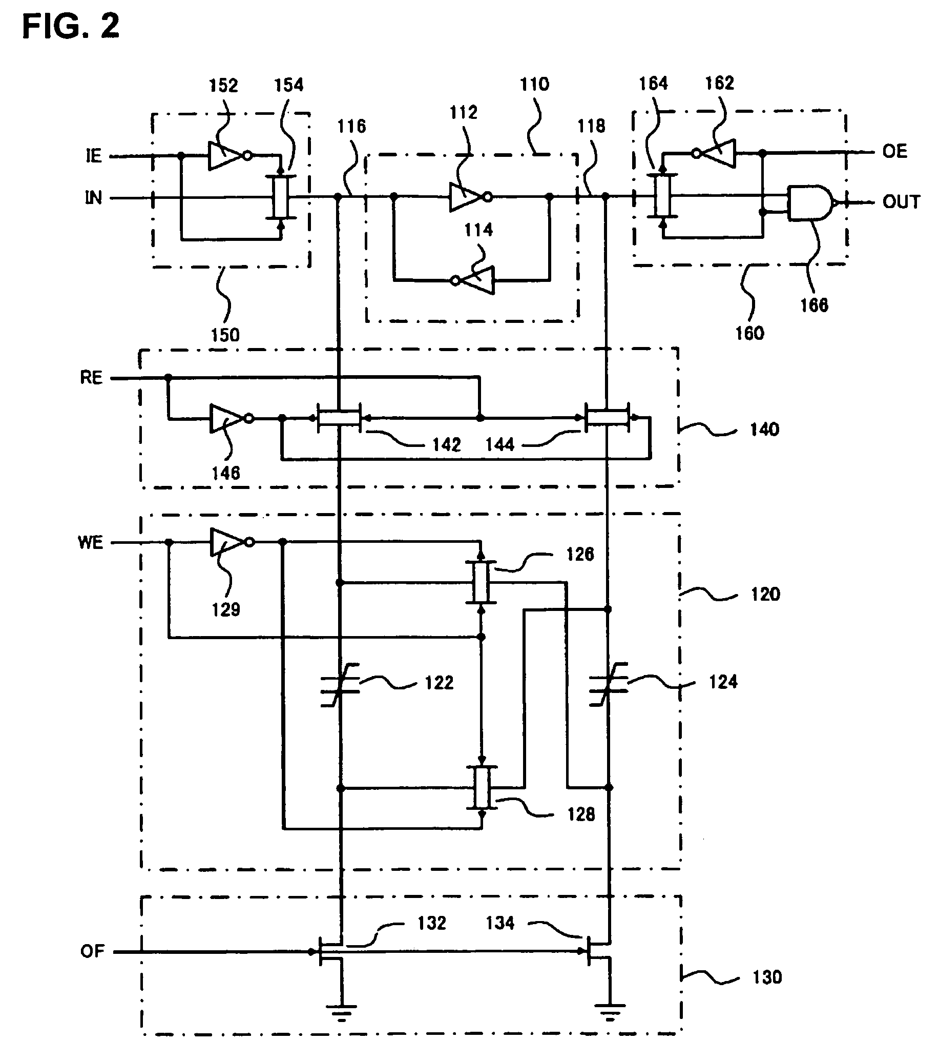
[0031]FIG. 2 is a diagram indicating the program circuit 100 in accordance with the The program circuit 100 has a structure equipped with a flip-flop 110, a storage section 120, a discharge section 130, a connecting section 140, a write section 150, and an output section 160. The program circuit 100 is a circuit that reads memory data stored in the storage section 120 that is a nonvolatile storage device, writes the memory data read out in the flip-flop 110, to thereby supply the memory data externally as an output signal OUT.
[0032]The flip-flop 110 is an example of a potential difference supply section, and is formed from a first inverter 112 and a second inverter 114, and a first terminal 116 and a second terminal 118 which electrically connect the flip-flop 110 to an external component. Each of the first inverter 112 and the second inverter 114 has an input terminal and an output terminal, wherein the output terminal of the first inverter 112 is electrically connected to the inp...
third embodiment
[0073]The program circuit 100 in accordance with the third embodiment differs from the other embodiments in the structure of its flip-flop 110. In the present embodiment, a first inverter 112 and a second inverter 114 that compose the flip-flop 110 are clocked inverters. Also, the control section 540 supplies to the flip-flop 110 a control signal FFE that is a signal to control operations of the first inverter 112 and the second inverter 114. Also, the program circuit 100 is further equipped with a seventh inverter 111 that receives the control signal FFE as an input, and supplies an inverted signal of the control signal to the first inverter 112 and the second inverter 114.
[0074]In the present embodiment, the first inverter 112 and the second inverter 114 are structured such that, when the logical value of the control signal FFE is logical H, signals received as inputs are inverted and outputted; and when the logical value of the control signal FFE is logical L, their outputs becom...
PUM
 Abstract
Description
Claims
Application Information


