Switch
- Summary
- Abstract
- Description
- Claims
- Application Information
AI Technical Summary
Benefits of technology
Problems solved by technology
Method used
Image

Examples
embodiment 1
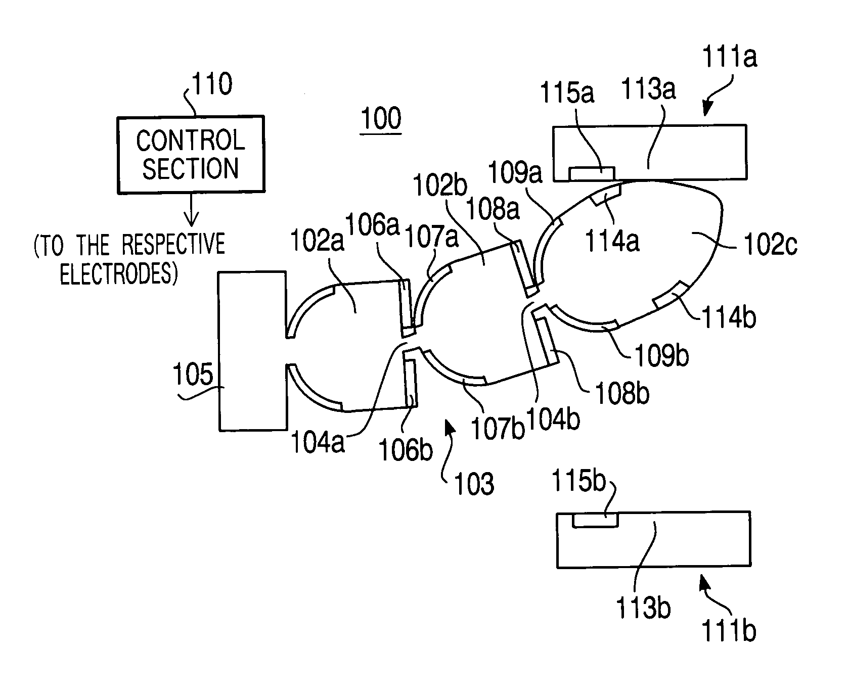
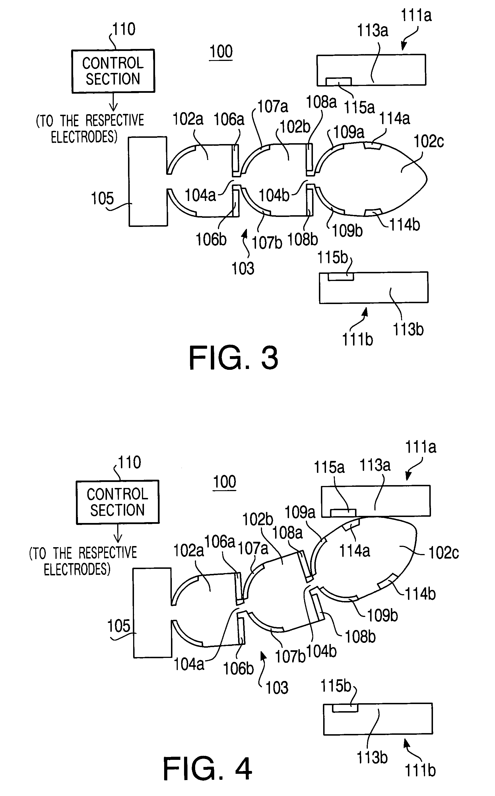
[0035]FIG. 3 is a plan view showing the configuration of a switch in accordance with embodiment 1 of the present invention. The switch 100 shown in FIG. 3 includes a microstructure group 103 including a plurality of microstructures 102a, 102b and 102c, forming an SPDT switch which moves on the substrate in the planar direction. This switch 100 is formed on a semiconductor integrated circuit by the same process as the integrated circuit and used in the transmitter circuit, the receiver circuit, the transmission / reception switching circuit of a wireless communication device, or in some circuits of a variety of other devices.
[0036]The microstructures 102a, 102b and 102c are made of polysilicon which makes it possible to firmly form an electrode on their surfaces, with an insulating film formed over the surface of the silicon. However, the present invention is not limited thereto, but can be practiced by the use of a polymer base material such as polyimide, or a silicon base material (S...
embodiment 2
[0073]FIG. 12 is a perspective view showing the configuration of a switch 200 in accordance with an embodiment 2 of the present invention. However, like reference numerals indicate similar elements as illustrated in FIG. 3 to FIG. 6, and detailed explanation will be omitted.
[0074]The switch 200 as shown in FIG. 12 is formed on a semiconductor integrated circuit by the same process as the integrated circuit and used in the transmitter circuit, the receiver circuit, the transmission / reception switching circuit of a wireless communication device, or in some circuits of a variety of other devices. In contrast to the two-dimensional travel (pivoting motion) of the above switch 100 as described in conjunction with FIG. 3, this switch 200 differs in the three-dimensional travel (pivoting motion). In order to realize the pivoting motion in the three-dimensional direction, this switch 200 has a microstructure group 203 as a movable member having a first microstructure 202a pivotally supporte...
embodiment 3
[0085]FIG. 16 is a side view showing the configuration of a switch 300 in accordance with an embodiment 3 of the present invention. The switch 300 as shown in FIG. 16 is formed on a semiconductor integrated circuit by the same process as the integrated circuit and used in the transmitter circuit, the receiver circuit, the transmission / reception switching circuit of a wireless communication device, or in some circuits of a variety of other devices. This switch 300 includes, as a movable member, microstructure groups 303 and 304 having the microstructures 301a, 301b, 301c, 302a, 302b and 302c in place of the microstructures 102a, 102b and 102c of the above switch 100 as shown in FIG. 3.
[0086]The microstructure group 303 is formed by linking the respective microstructures 301a, 301b and 301c by the linking beams 305 with its fixed end linked to a fixed member 306 fixed to a substrate (not shown in the figure) approximately at the right angle and its movable end linked to a movable memb...
PUM
 Abstract
Description
Claims
Application Information
 - Generate Ideas
- Intellectual Property
- Life Sciences
- Materials
- Tech Scout
- Unparalleled Data Quality
- Higher Quality Content
- 60% Fewer Hallucinations
Browse by: Latest US Patents, China's latest patents, Technical Efficacy Thesaurus, Application Domain, Technology Topic, Popular Technical Reports.
© 2025 PatSnap. All rights reserved.Legal|Privacy policy|Modern Slavery Act Transparency Statement|Sitemap|About US| Contact US: help@patsnap.com