
Universal spatial pattern recognition system

a spatial pattern recognition and data format technology, applied in semiconductor/solid-state device testing/measurement, image enhancement, instruments, etc., can solve the problems of limited “eyeball” technique, inability to provide information on the manufacturing process, and inability to achieve spatial analysis. to achieve the effect of maximizing the effectiveness of a spatial analysis system

Active Publication Date: 2006-09-12
ADVANCED MICRO DEVICES INC
View PDF16 Cites 28 Cited by
  • Summary
  • Abstract
  • Description
  • Claims
  • Application Information

AI Technical Summary

Benefits of technology

[0008]Accordingly, it is desirable to produce a method for automating the wafer test bin in processing of manufacturing faults on semiconductor wafers to generate a representative wafer map showing meaningful fault patterns to maximize the effectiveness of a spatial analysis system wherein all types of patterns associated numeric outputs are evaluated in or by a common platform.

Problems solved by technology

Semiconductor wafer fabrication involves complex manufacturing processes to produce integrated circuits on the surface of silicon wafers.
Generally, random fault patterns do not provide information on the manufacturing process that can be used to enhance the yield.
This “eyeball” technique is limited because the analysis is done only on selected sample wafers.
This manual technique is labor intensive and time consuming.
Moreover, it does not provide data storage for correlating with future test data.

Method used


Image

  • Universal spatial pattern recognition system
  • Universal spatial pattern recognition system
  • Universal spatial pattern recognition system

Examples


Embodiment Construction

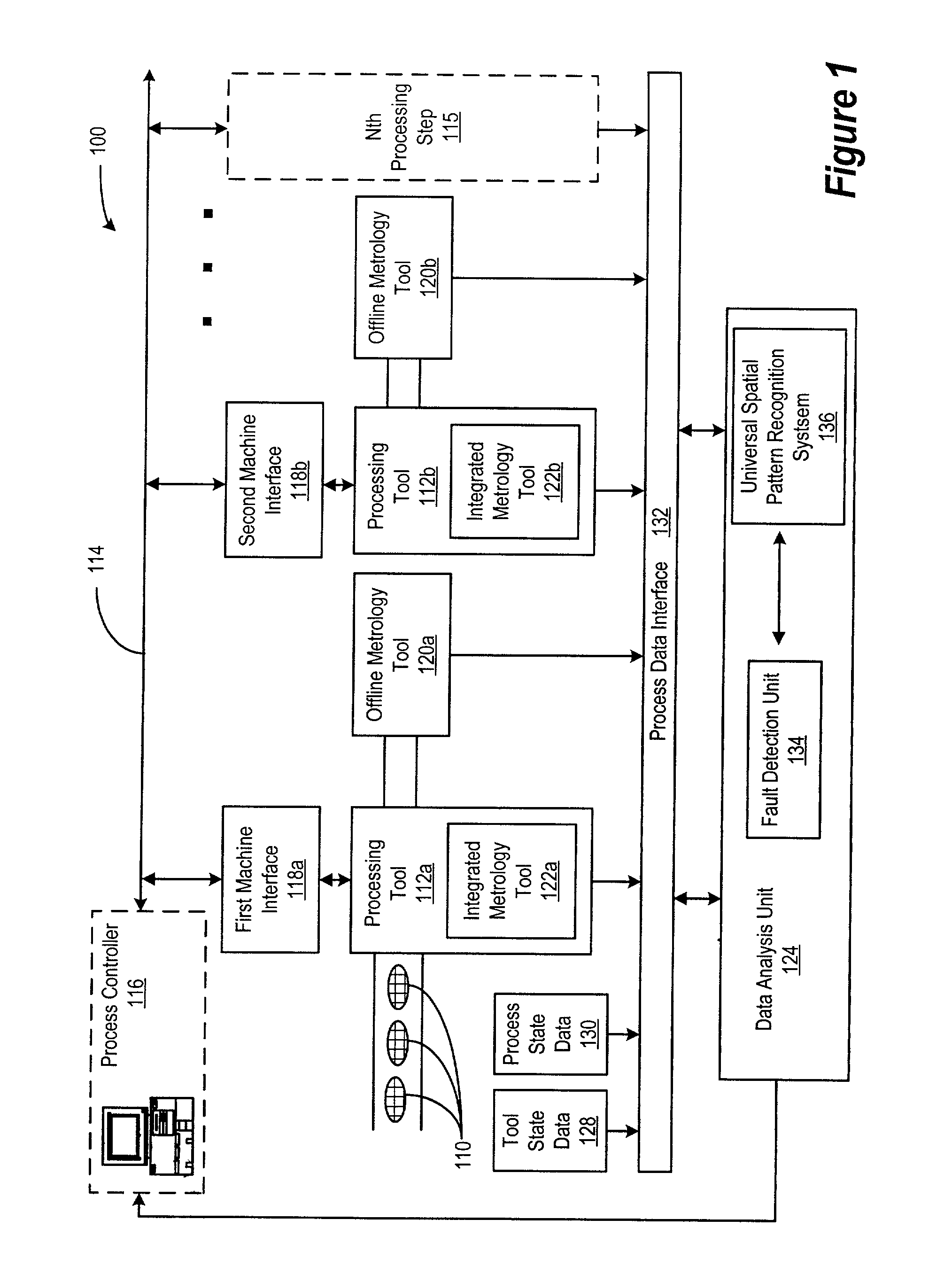
[0019]FIG. 1 is a block diagram of a semiconductor manufacturing line 100 that illustrates the process environment in which the Universal Spatial Pattern Recognition system of the present invention operates. Semiconductor wafers 110 are processed on processing tools 112a, 112b using a plurality of control input signals, or manufacturing parameters, provided by a computerized process controller 116 via a network 114. Control input signals or manufacturing parameters are sent to the processing tools 112a, 112b from the computerized process controller 116 via machine interfaces 118a, 118b. The first and second machine interfaces 118a, 118b are located outside the processing tools 112a, 112b. In an alternative embodiment, however, the first and second machine interfaces 118a, 111b can be located within the processing tools 112a, 112b. The semiconductor wafers 110 may be provided to the processing tools 112a, 112b in an automatic fashion (e.g., robotic movement of semiconductor wafer 110...


PUM


Abstract

A method and apparatus for analyzing patterns in semiconductor wafers wherein the patterns are compared to a plurality of patterns stored in a common pattern library. A spatial pattern recognition engine is operable to receive a first set of data corresponding to a pattern on a semiconductor wafer and to generate a normalized contour representation of said first data set. A pattern analyzer compares the normalized data set to a plurality of reference contour data sets stored in a common pattern data reference library and generates a correlation label associating the first data set with one of the plurality of reference contour data sets. The label associated with the first data set is stored in a label storage database that can be accessed to perform subsequent analysis on the data associated with a specific wafer. The system can be used to analyze multiple types of patterns, including defect data, bin data, positional parameter data and in-line site data.

Description

BACKGROUND OF THE INVENTION[0001]1. Field of the Invention[0002]The present invention relates to the field of semiconductor manufacturing and, more particularly, to a system for universal spatial pattern recognition of data formats on semiconductor wafers.[0003]2. Description of the Related Art[0004]Semiconductor wafer fabrication involves complex manufacturing processes to produce integrated circuits on the surface of silicon wafers. In order to characterize the quality of a wafer, each die is associated with a wafer test bin containing an alphanumeric code that represents the type of functional and non-functional die. The collective wafer test bins are grouped to generate a bin summary or a wafer map showing the locations of faulty dice and the type of manufacturing faults associated with these dice.[0005]A goal of semiconductor manufacturing is to attain a high yield rate from all wafers during the device lifetime. Generally, random fault patterns do not provide information on th...

Claims


Application Information

Patent Timeline
Patent Type & Authority Patents(United States)
IPC IPC(8): G06K9/00G06V10/46
CPCG06K9/48G06T7/0006G06K9/6292G06T2207/30148G06V10/46G06F18/254
Inventor MCINTYRE, MICHAEL G.MORRIS, JAMES E.
Owner ADVANCED MICRO DEVICES INC
Learn More