Method of manufacturing an ultra-miniature magnetic device

a magnetic device, ultra-miniaturized technology, applied in the direction of magnetic bodies, semiconductor/solid-state device details, instruments, etc., can solve the problems of inability to manufacture a machine with these small cores, and inability to meet the requirements of the circui

Inactive Publication Date: 2006-09-19
BH ELECTRONICS
View PDF31 Cites 71 Cited by
  • Summary
  • Abstract
  • Description
  • Claims
  • Application Information

AI Technical Summary

Benefits of technology

[0050]FIG. 19L illustrates removing excess seed layer material to avoid shorting between adjacent magnetic devices.

Problems solved by technology

However, a problem with conventional magnetic components is that they are large and bulky in comparison to the circuits in which they operate.
Machine assembly with these small cores is impractical.
Because all of these operations require high levels of manual dexterity and are very time consuming, it is not uncommon for labor costs to represent 60–70% of the total product cost.
However, since this research generally applies to sensors and higher power magnetic devices operating in lower frequency ranges, the research is generally not applicable or viable for high frequency applications.

Method used


Image

  • Method of manufacturing an ultra-miniature magnetic device
  • Method of manufacturing an ultra-miniature magnetic device
  • Method of manufacturing an ultra-miniature magnetic device

Examples


Embodiment Construction

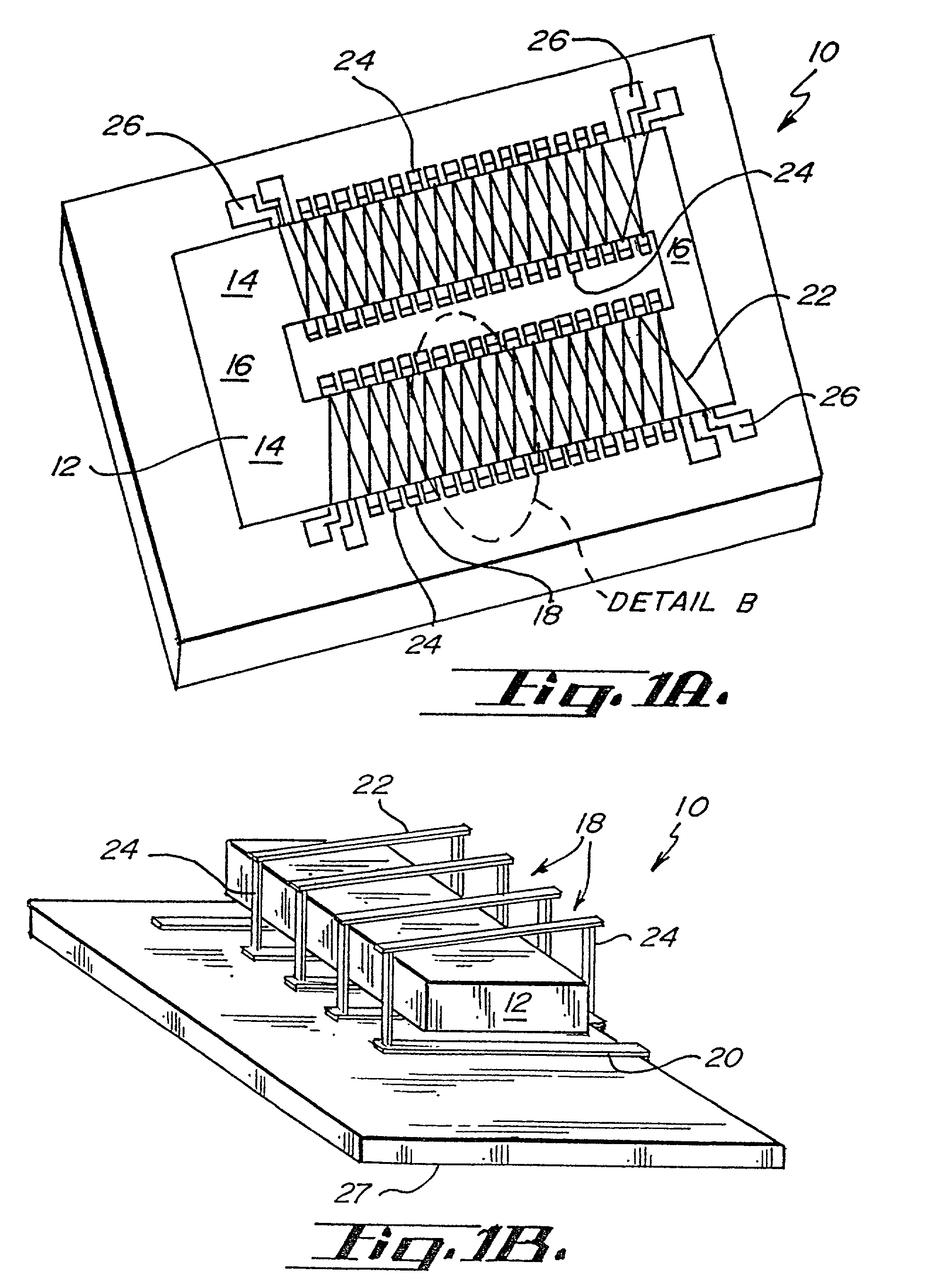
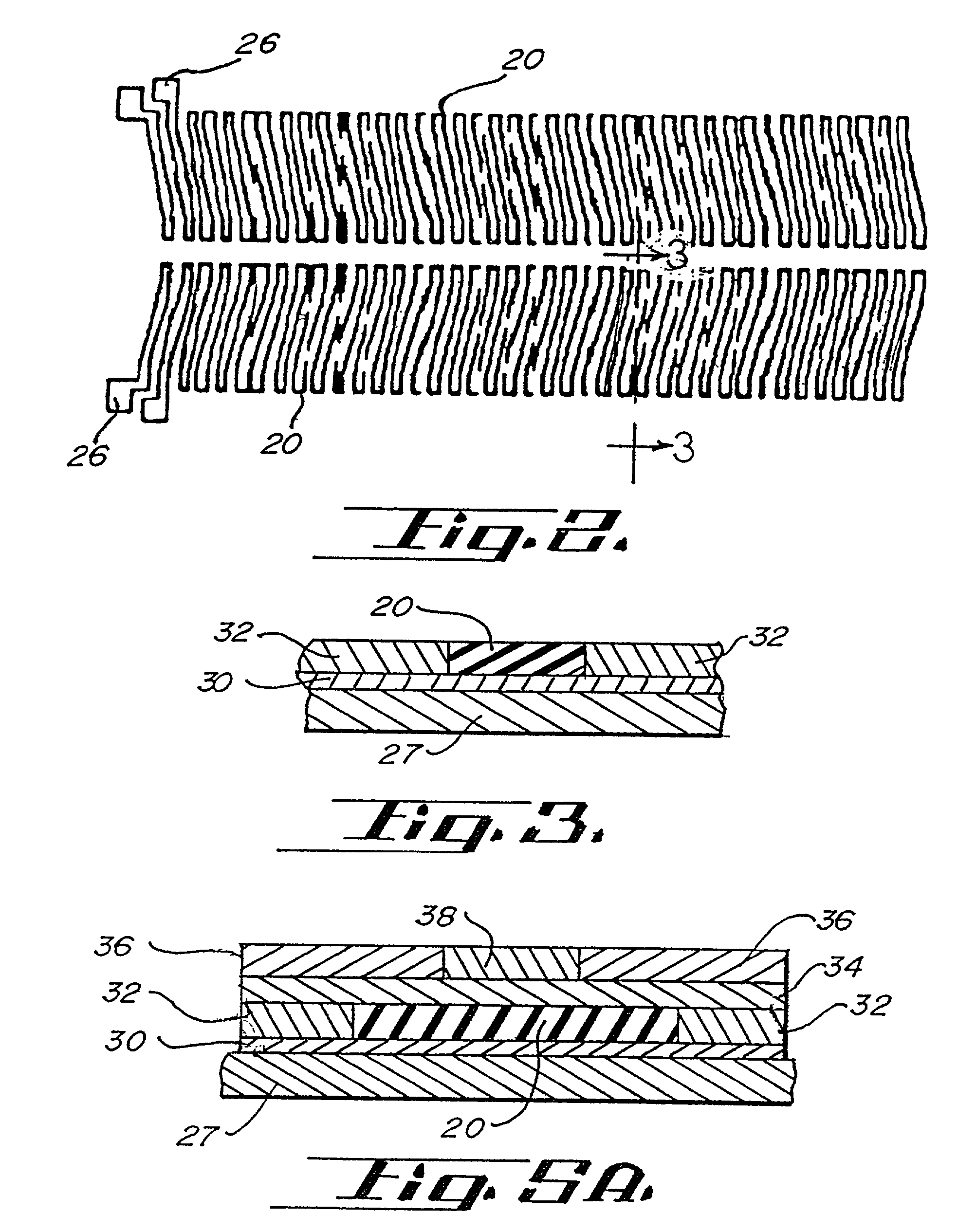
[0051]An ultra-miniature magnetic device 10 of the present invention is depicted in FIGS. 1A–B. As shown, device 10 generally includes a magnetic core 12, which is preferably in the configuration of an elongated rectangle or oval having two elongate sides 14 and two short sides 16, and a coil winding 18, which is preferably comprised of a lower conductor 20 and an upper conductor 22 connected by conducting vias 24. Bonding pads 26 are provided on coil winding 18 for connection to external circuitry. Ultra-miniature magnetic device 10 is preferably fabricated atop a silicon substrate 27 although other possible substrates such as glass, fiberglass, polyimide, ceramics and other insulating materials can be used.

I. Fabrication of Ultra-Miniature Magnetic Device

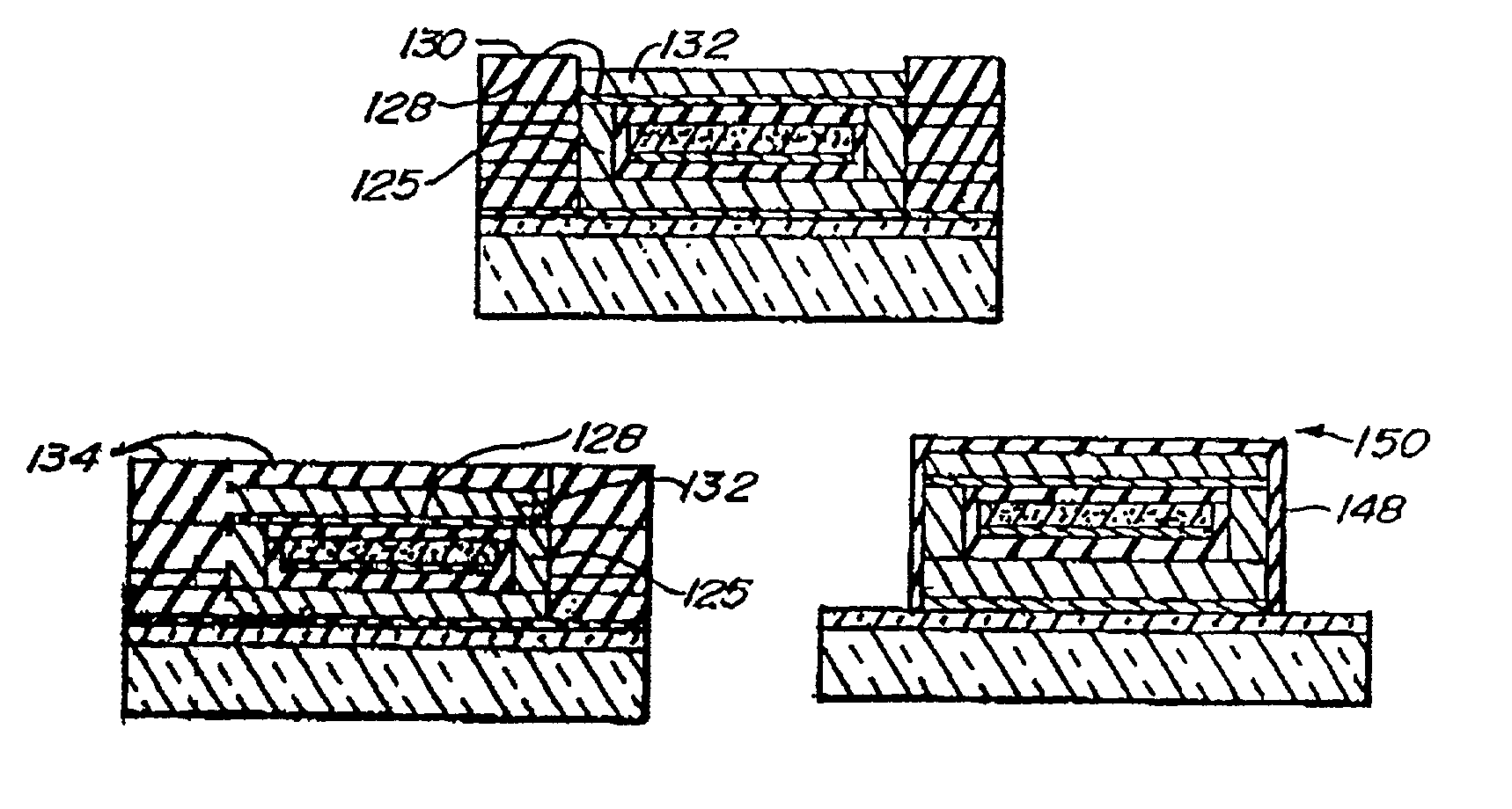
[0052]Device 10 is preferably fabricated using automated, semiconductor fabrication processes. In general, four main stages define the fabrication process: (1) Creation of lower conductor 20; (2) Addition of magnetic core 12; (3) ...


PUM

PropertyMeasurementUnit
frequencyaaaaaaaaaa
diametersaaaaaaaaaa
sizesaaaaaaaaaa

Abstract

An ultra-miniature magnetic device generally comprises a conductive winding and a magnetic core. The conductive winding includes an upper conductor and a lower conductor. The magnetic core is of an elongate rectangular or oval shape having two elongate sections and two short sections. The lower conductor is preferably positioned below the elongate sections of the magnetic core while the upper conductor is preferably positioned above the elongate sections of the magnetic core. The lower and upper conductors are electrically connected by conducting via structures that are formed in sequential steps using semiconductor processing technology. The result is a coil winding around the elongate sections, with the short sections being preferably free of windings. The process provides an advantage of avoiding shorting between the via structures and the magnetic core caused by overetching when etching the via holes.

Description

RELATED APPLICATIONS[0001]The present application is a continuation-in-part of application Ser. No. 09 / 530,371 filed on Apr. 27, 2000, now abandoned, which claims priority from the PCT Application filed on Jul. 23, 1999, having Ser. No. PCT / US99 / 16446 which claims priority from U.S. Provisional Application having Ser. No. 60 / 093,824, filed Jul. 23, 1998, which are hereby incorporated by reference in their entirety.FIELD OF THE INVENTION[0002]The present invention relates to transformers and inductors fabricated with high volume semiconductor technology production processes.BACKGROUND OF THE INVENTION[0003]High frequency magnetic components are used in many applications including computer data transmission, cable TV video, and interactive CATV, among others. These applications generally require transformers and inductors that operate efficiently in the frequency range from 5 MHz to 1 GHz and beyond. However, a problem with conventional magnetic components is that they are large and b...

Claims


Application Information

Patent Timeline
Patent Type & Authority Patents(United States)
IPC IPC(8): H01F7/06G11B5/17H01F17/00H01F41/04H01F41/34H01L23/64
CPCH01F17/0006H01F41/046H01F41/34H01L23/645H01F17/0033Y10T29/49073H01L2924/09701H01L2924/0002Y10T29/49062Y10T29/4902Y10T29/49156Y10T29/49165Y10T29/49064H01L2924/00
Inventor HIATT, FRED C.DECRAMER, JOHN E.FAYFIELD, ROBERT T.RASSEL, RICHARD J.
Owner BH ELECTRONICS
Why Eureka
Try Eureka