Magnetic field enhanced photovoltaic device

a photovoltaic device and magnetic field technology, applied in thermoelectric devices, solid-state devices, magnetic bodies, etc., can solve the problems of the biggest bottleneck in the production of photovoltaic devices, the inability to produce photovoltaic devices, etc., to reduce internal resistance, reduce scattering probability, and enhance the efficiency of photovoltaic devices

Active Publication Date: 2006-09-19
IND TECH RES INST
View PDF18 Cites 16 Cited by
  • Summary
  • Abstract
  • Description
  • Claims
  • Application Information

AI Technical Summary

Benefits of technology

[0005]The invention incorporates a magnetic field to enhance the efficiency of the photovoltaic device. The additional magnetic field in the photovoltaic device will polarize the spin state of electrons that migrate inside the photovoltaic device. For example, a ferro-antiferromagnetic layer interfacing with a coupling layer produces an exchange coupling effect and pins the spin state of electrons, which reduces scattering probability during electron transmission, reduces internal resistance and increases conversion efficiency.
[0006]An electron possesses two intrinsic characteristics: charge and spin, which can be considered as smallest units for electricity and magnetism. In the traditional design of a photovoltaic device, only the effect of electron's charge characteristic is considered while its spin characteristic is overlooked. Due to the latest development in nano-technology, it has become feasible to control the spin of electrons to reduce resistance and improve efficiency. The characteristic of magnetic resistance is stated in differential spin scattering theory, that is, when the spin direction of migrating electrons is parallel to that of the conducting material they are migrating through, and the probability of electron scattering is reduced. Therefore, a photovoltaic device incorporated with a magnetic field can change its overall magnetic resistance, a phenomenon called “magnetic resistance.” The combination of ferro-magnetic and ferro-antiferromagnetic layers can produce an exchange coupling effect, in which the spin state of nearby migrating-through electrons is pinned by the anti-ferromagnetic layer.
[0007]A magnetic photovoltaic device, based on the above-mentioned theory to increase the photoelectric conversion efficiency, includes a photoelectric conversion layer, a first electrode, a second electrode, a ferro-antiferromagnetic exchange coupling layer and an applied magnetic field. The first electrode and the second electrode are respectively disposed on two surfaces of the photoelectric conversion layer to collect electrons and holes generated by the photoelectric conversion layer. The first electrode is pervious to light, which reaches to the photoelectric conversion layer through the first electrode, where the light energy is converted into electron-hole pairs. In the meantime, the applied magnetic field polarizes the spin state of electrons, and the ferro-antiferromagnetic exchange coupling layer adjoining the photoelectric conversion layer produces an exchange coupling effect, which creates extra magnetic bias on the junction and pins the spin state of electrons and further fixes the spin direction of electrons. Thus, if the spin directions of electrons are parallel to the direction of the magnetic field, the electron transmission resistance can be greatly reduced and its diffusion length increased. The process reduces the recombination probability of electrons and holes and hence increases photoelectric conversion efficiency. Hence, an additional hard magnetic layer in photovoltaic device provides the needed magnetic field and ensures the spin directions of electrons are the same as the direction of the magnetic field.

Problems solved by technology

In the laboratory, the photovoltaic device can almost reach the highest light-electricity-conversion level theoretically allowed, but in reality due to the complexity of the mass manufacturing process cost-effective high-efficient photovoltaic devices cannot be produced.
Currently, this is the biggest bottleneck in making photovoltaic devices.

Method used


Image

  • Magnetic field enhanced photovoltaic device
  • Magnetic field enhanced photovoltaic device
  • Magnetic field enhanced photovoltaic device

Examples


Embodiment Construction

[0012]Reference will now be made in detail to the preferred embodiments of the invention, examples of which are illustrated in the accompanying drawings. Wherever possible, the same reference numbers are used in the drawings and the description to refer to the same or like parts.

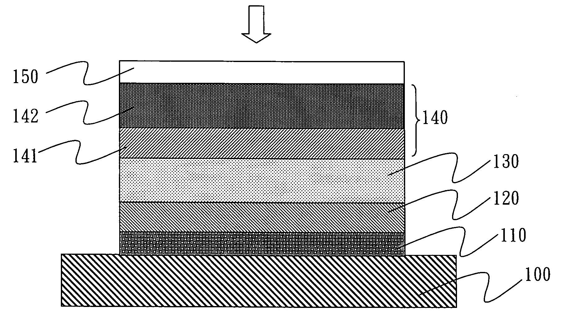
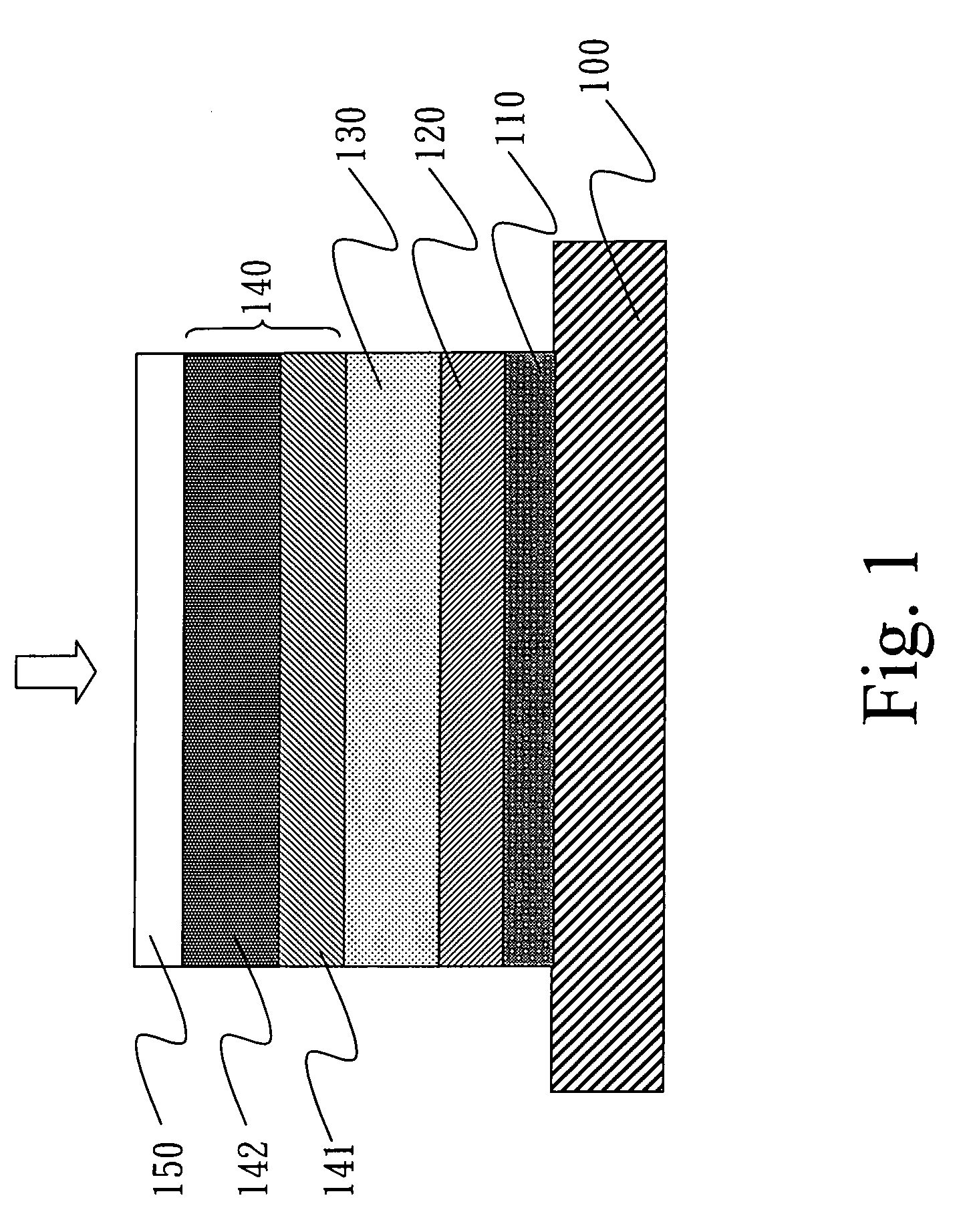
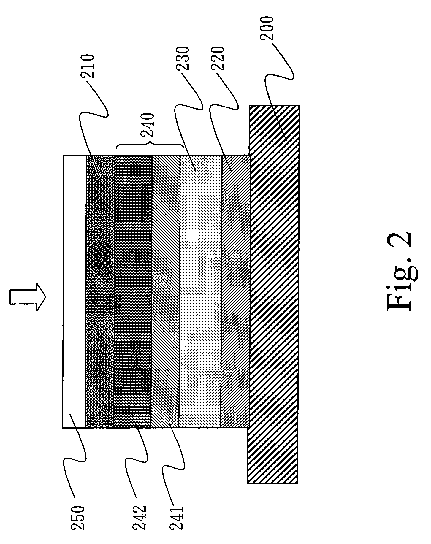
[0013]A magnetic field enhanced photovoltaic device of invention can be applied to all kinds of photovoltaic devices, no matter what material is used, e.g., Single Crystal, Polycrystal, Amorphous, or Quantum dot, Nano-Wire, Nano-Rod and Qunatum Well arranged with nanocrystal.

[0014]For different kinds of photovoltaic devices, such as P-N semi-conductor solar battery, nano-rod solar battery or dye photoactivated solar battery, their photoelectric conversion layers can be P-N junction semi-conductor layers, a nano-rod and high polymer mixed layer or a photoactivated layer. The first electrode has to be pervious to light, so conducting glass having a layer of FTO, ITO or IZO, etc., is used for the layer. Because...


PUM


Abstract

A magnetic field enhanced photovoltaic device includes a photoelectric conversion layer, a first electrode, a second electrode, a ferro-antiferromagnetic exchange coupling layer and an applied magnetic field. The first electrode and the second electrode are respectively disposed on two surfaces of the photoelectric conversion layer to collect electrons and holes generated by the photoelectric conversion layer. The first electrode is pervious to light. The incident light reaches the photoelectric conversion layer through the first electrode. The applied magnetic field polarizes the spin state of electrons. The ferro-antiferromagnetic exchange coupling layer adjoins the photoelectric conversion layer and pins the spin state of electrons.

Description

FIELD OF THE INVENTION[0001]The invention relates to a photovoltaic device, and particularly to a magnetic field enhanced photovoltaic device.BACKGROUND OF THE INVENTION[0002]A photovoltaic device (including a solar energy battery) is different from the regular battery. A photovoltaic device converts light into electrical energy, its P-N junction structure when exposed to incident light generates large quantities of electron-hole pairs, and in the meantime electrons carrying negative electricity and holes carrying positive electricity migrate to the N-type semi-conductor and P-type semi-conductor respectively. This process produces electricity.[0003]During the conversion process, not all the incident sun-light can be absorbed and converted to electricity by the photovoltaic device. One section of the light spectrum does not contribute to the battery's output due to its low energy (which should be greater than semi-conductor's energy gap). When the photovoltaic device receives light ...

Claims


Application Information

Patent Timeline
Patent Type & Authority Patents(United States)
IPC IPC(8): H01L31/04H01L31/0216
CPCB82Y25/00H01F10/3218H01L31/0352H01L51/4213H01L51/4266H01L31/06Y02E10/549H10K30/10H10K30/352H10K30/50
Inventor CHU, CHIA-FAN
Owner IND TECH RES INST
Why Eureka
Try Eureka