Method and system for single-chip camera

a single-chip camera and camera body technology, applied in the field of single-chip image and video camera, can solve the problems of non-optimal form factor and power consumption, and achieve the effects of low power consumption, cost effective, and small siz

Inactive Publication Date: 2006-09-26
PHOTONIC IMAGING SOLUTIONS INC
View PDF3 Cites 47 Cited by
  • Summary
  • Abstract
  • Description
  • Claims
  • Application Information

AI Technical Summary

Benefits of technology

[0044]The present invention provides single-chip cameras that are small in size, cost effective and require low power consumption, the cameras are thereby ideal for applications where space and low power consumption are critical.
[0045]Therefore, the present invention is proposed to compact as many functional elements as possible into a single IC so that the product size is smaller, the interface is simpler, the power consumption is lower, and the cost is lower.

Problems solved by technology

Such designs requires tremendous amount of collaborative effort to establish communications between different chips, and therefore is non-optimal in terms of form factor and power consumption.

Method used


Image

  • Method and system for single-chip camera
  • Method and system for single-chip camera
  • Method and system for single-chip camera

Examples


Embodiment Construction

[0053]The following description is presented to enable one of ordinary skill in the art to make and use the invention and is provided in the context of a patent application and its requirements. In the following description, specific nomenclature is set forth to provide a thorough understanding of the present invention. It will be apparent to one skilled in the art that the specific details may not be necessary to practice the present invention. Furthermore, various modifications to the embodiments will be readily apparent to those skilled in the art and the generic principles herein may be applied to other embodiments. Thus, the present invention is not intended to be limited to the embodiments shown but is to be accorded the widest scope consistent with the principles and features described herein.

Architecture:

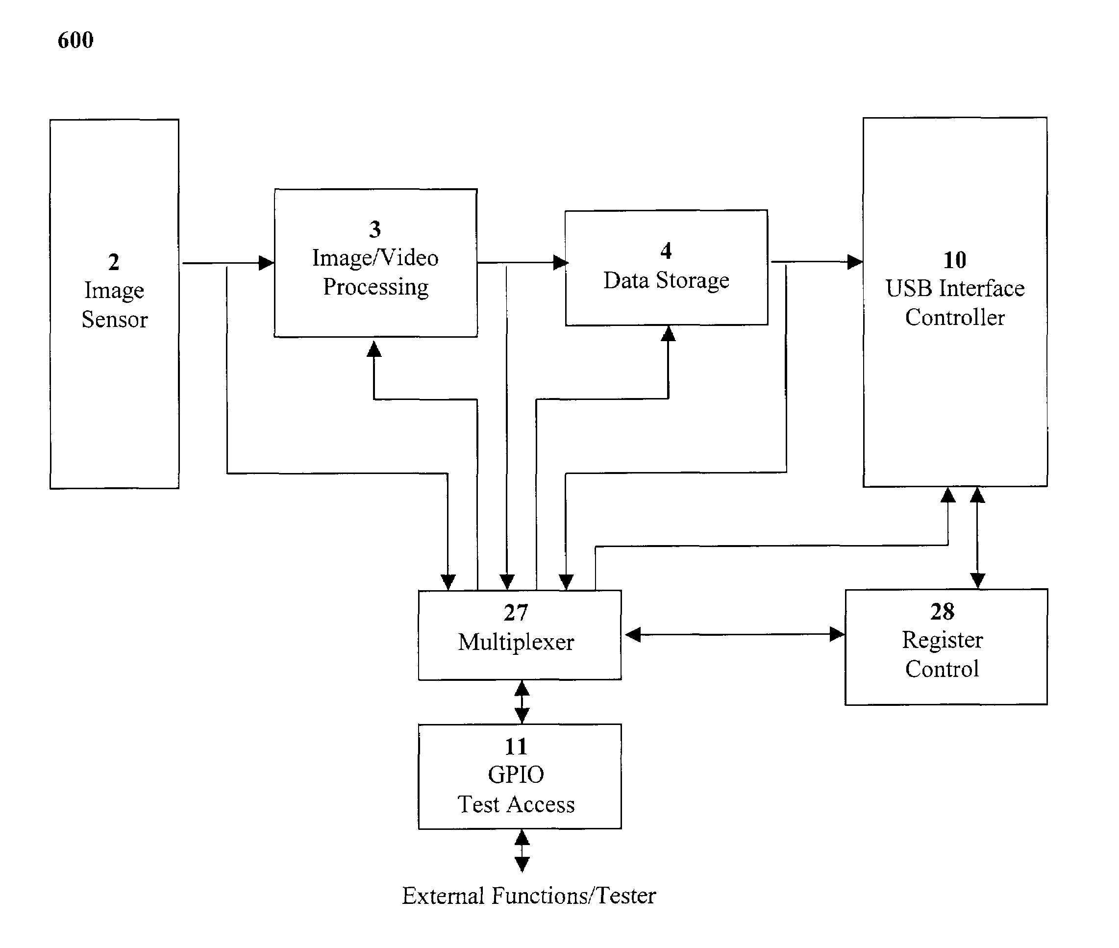
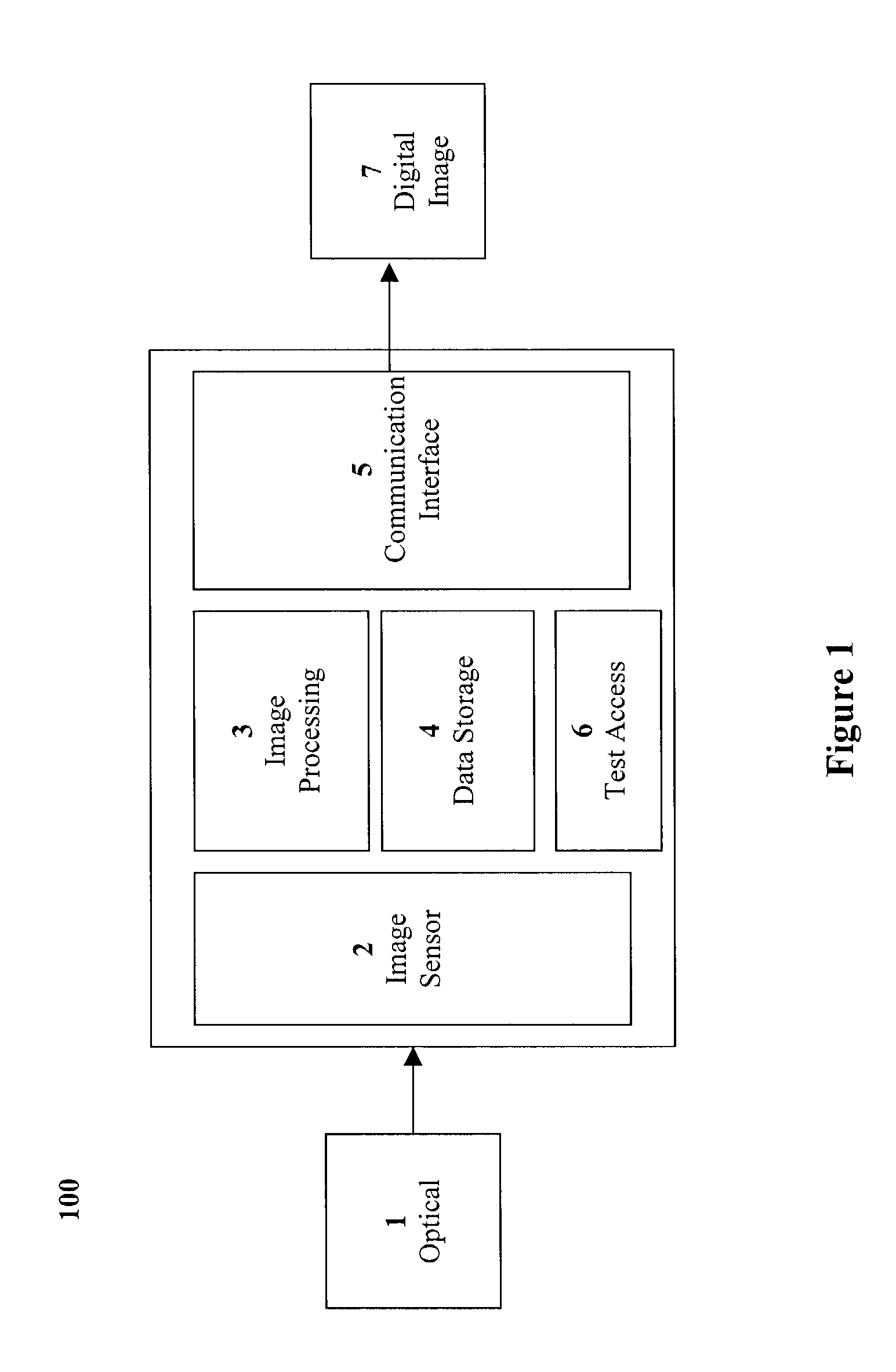
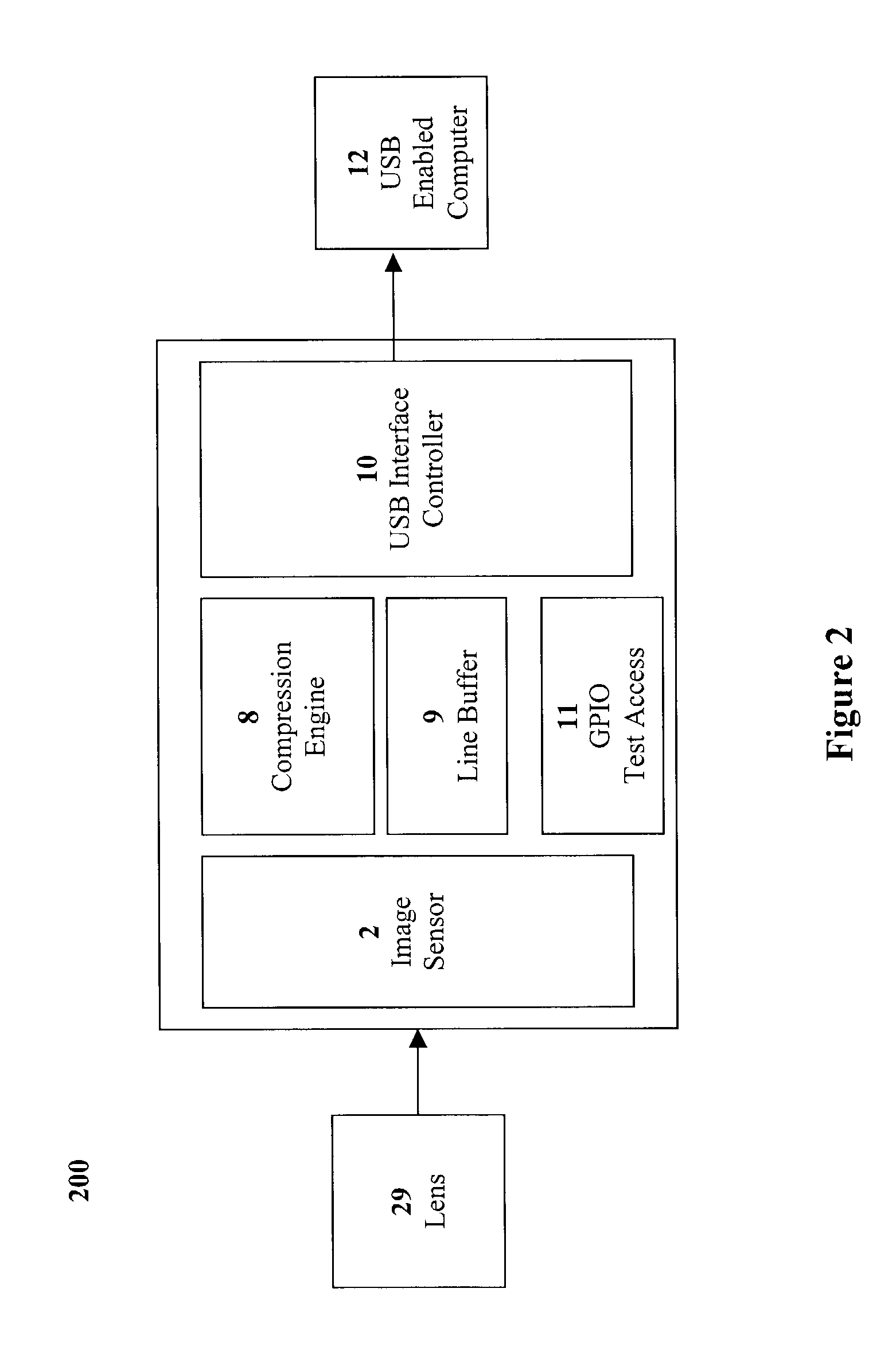
[0054]FIG. 1 is a block diagram illustrating a system 100 comprising a single-chip camera in accordance to one embodiment of the present invention. System 100 comprises: an ...


PUM


Abstract

Method and system for a single-chip camera where an image sensor is a single-chip digital color imaging device that incorporates a sensor array that captures still or full-motion video and converts the images to digital data. Moreover, the image sensor employs a built-in correlated double sampler, an internal analog-to-digital converter, and a timing circuitry. Output from the sensor is an 8-bit or more raw data, horizontal sync signals, and vertical sync signals. The output raw data may then be fed into a compression circuit that generates packets of compressed output data. The compressed data is transmitted with a USB transceiver using isochronous packets. The packets are then received, decompressed, and color processed by a host PC.

Description

BACKGROUND INFORMATION[0001]1. Field of Invention[0002]The present invention relates to the field of color imaging devices, and particularly to single-chip image and video camera.[0003]2. Description of Related Art[0004]Traditional cameras use film to store images. Analogously, a digital camera uses a solid state device called an image sensor to store images.[0005]Image sensors are built on silicon chips containing millions of photosensitive diodes named photocells. Each photocell records the intensity of brightness of light shone on the photocell.[0006]Moreover, each photocell reacts to light by accumulating a charge that directly corresponds to the brightness of the light. The brightness recorded is then converted to a set of numbers that can be used to digitally save the image and set the color and brightness of pixels on the screen or ink on printed page to reconstruct the image.[0007]A Charge-Coupled Delay (CCD) sensor uses a non-standard semiconductor process to manufacture th...

Claims


Application Information

Patent Timeline
Patent Type & Authority Patents(United States)
IPC IPC(8): H04N5/225H04N17/02
CPCH04N17/002
Inventor WU, BEN S.CAPE, JAMESLIN, SHANG-HUNG
Owner PHOTONIC IMAGING SOLUTIONS INC
Why Eureka
Try Eureka