Device, system, server, client, and method for supporting component layout design on circuit board, and program for implementing the device

a technology for circuit boards and components, applied in the field of devices, systems, servers, clients, etc., can solve the problems of system not considering and supporting the layout of elements, noise sources, and inability to completely eliminate nois

Active Publication Date: 2006-09-26
NEC CORP
View PDF18 Cites 26 Cited by
  • Summary
  • Abstract
  • Description
  • Claims
  • Application Information

AI Technical Summary

Benefits of technology

[0009]It is therefore an object of the present invention to provide a device and a method capable of supporting the layout design of main components such as LSI on a printed circuit board in which unnecessary electromagnetic radiation (interference) is suppressed.

Problems solved by technology

The error displaying section 128 displays an error when it is impossible to mount a bypass capacitor even when the wiring line has been relocated.
However, the above-described system has the following problem that it is impossible to completely eliminate noise that becomes resonance energy between a power source plane and a ground plane, the resonance energy also being a part of the reason for unnecessary electromagnetic radiation.
This is because, although the conventional system determines the position where a bypass capacitor will be located, the system does not consider and support a layout of an element, which may become a noise source, such as a large-scale integration (LSI).

Method used


Image

  • Device, system, server, client, and method for supporting component layout design on circuit board, and program for implementing the device
  • Device, system, server, client, and method for supporting component layout design on circuit board, and program for implementing the device
  • Device, system, server, client, and method for supporting component layout design on circuit board, and program for implementing the device

Examples


first embodiment

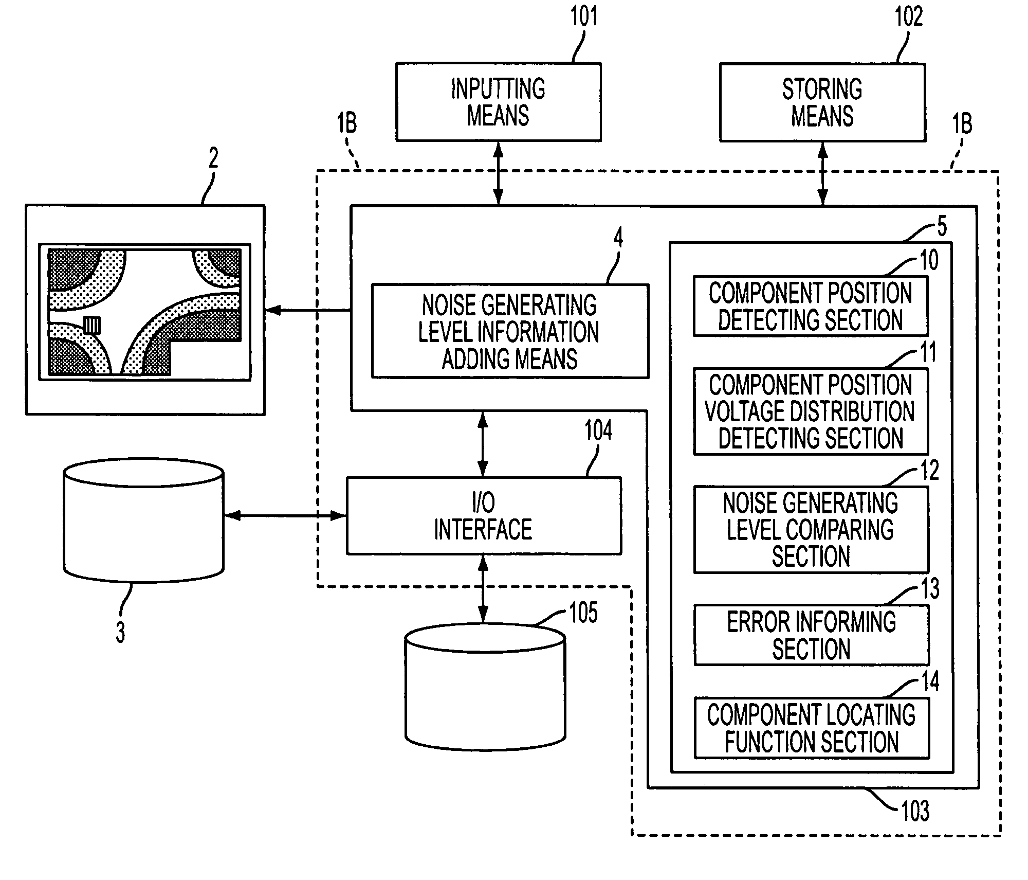
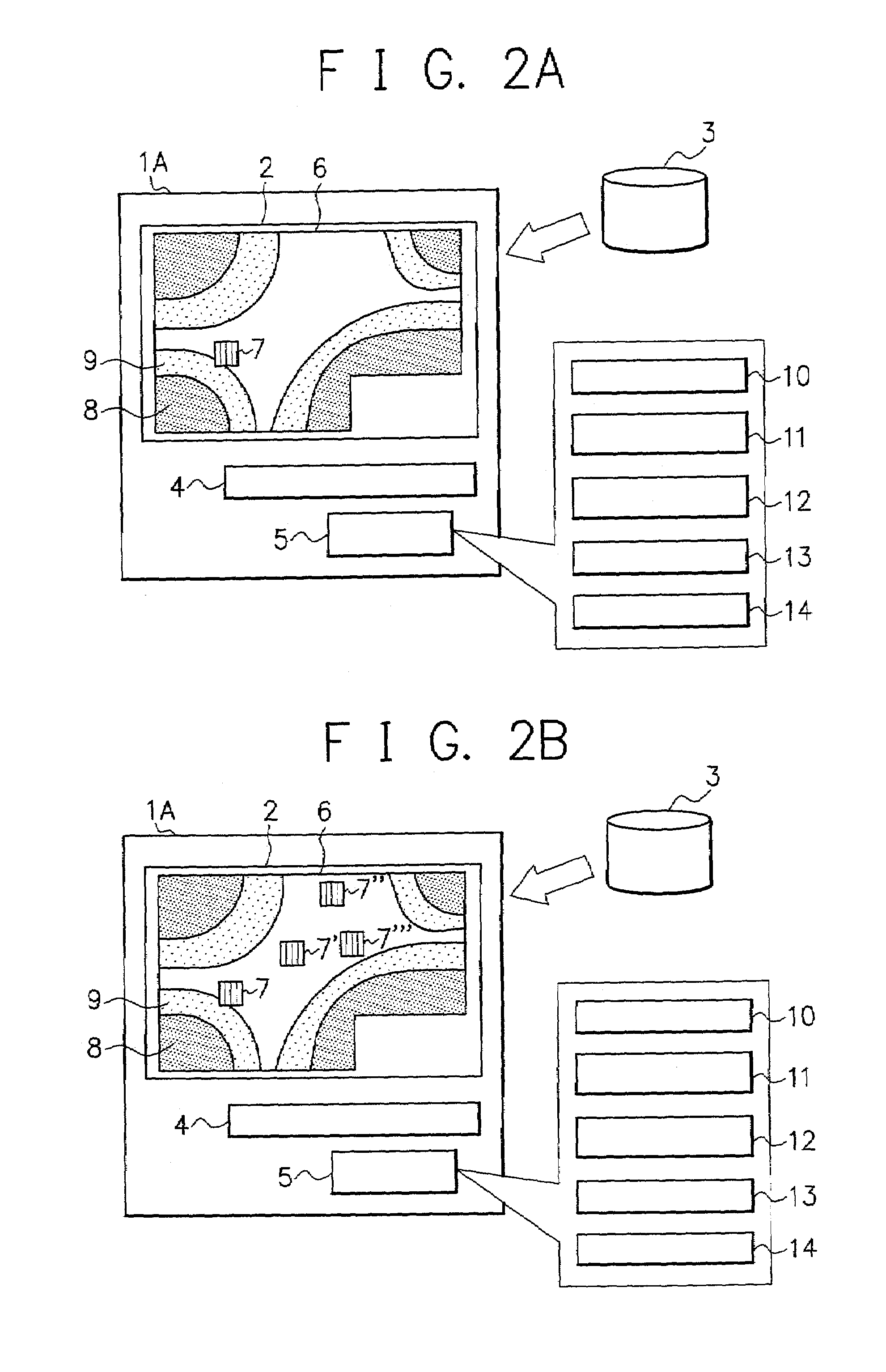
[0074]In this embodiment, the supporting device 1(A) for designing a layout of components (electronic components and microchips) on a circuit board shown in FIGS. 2A and 2B is configured as a standalone type. However, even when the device 1 is configured as a standalone type, the device 1 can be connected to the component library(ies), etc. via a network or by using a LAN adapter, etc., and thereby, it becomes possible to share the library(ies), etc. (including a database) easily among users.

[0075]FIG. 3 is a block diagram showing a configuration of the first embodiment of the present invention. As shown in FIG. 3, the device 1 for supporting a component layout design on a circuit board comprises a displaying section 2, a component library 3, an inputting means 101, a storing means 102, an arithmetic processing section 103, an I / O (input and output) interface 104, and a recording medium 105.

[0076]As shown in FIG. 3, the arithmetic processing section 103 includes the noise generating...

second embodiment

[0145]Next, an explanation will be given of a device, a system, a server, and a client for supporting designing a layout of electronic components and chips on a circuit board such as a printed circuit board, a method for supporting designing a layout thereof, and a program for realizing the device according to a second embodiment of the present invention referring to drawings.

[0146]While in the first embodiment whether or not noise (unnecessary electromagnetic radiation) arises is determined with respect to each component (microchips), the determination is executed with respect to each pin set to a component in the second embodiment. A noise source is generally found in a position where a pin(s) connecting each component to wiring is located on a printed circuit board. Thereby, the device in this embodiment is configured so as to identify a position of a pin that has the possibility of generating (creating) noise more precisely.

[0147]Referring to FIG. 13, an explanation will be give...

third embodiment

[0216]While in the above-described first and the second embodiment the circuit design supporting device 1 has the standalone configuration, the circuit design supporting device (system) in this embodiment has a configuration such that a component library (which is the same as the component library 3 or 30 in the first or second embodiment, respectively) is shared via a network. In the following, the configuration and the operation will be explained taking some examples.

[0217]FIG. 22 is a diagram showing a configuration of the circuit design supporting system according to this embodiment. As shown in FIG. 22, circuit design supporting terminals 201a, 201b, 201c, . . . , each of which serves as the circuit design supporting device 1 in the first or second embodiment, are connected to a network 200. Each of the circuit design supporting terminals 201a, 201b, 201c, . . . , is an electronic apparatus capable of being connected to the Internet, for example, an electron computer such as a ...


PUM


Abstract

There is provided a circuit design supporting device, a circuit board design supporting system, a circuit board design supporting server, a circuit board design supporting client, a circuit design supporting method, and a program for realizing the device for designing a layout of main components such as LSI, etc. on a circuit board such as a printed circuit board wherein unnecessary electromagnetic radiation is suppressed. The circuit design supporting device comprises a noise generating level adding means and a component locating means. The noise generating level adding means adds noise generating level information to a component to be located on a printed circuit board. The component locating means includes a component position detecting section, a voltage distribution detecting section, a noise generating level comparing section, and an error informing section. The component position detecting section detects a position of the component moved on the printed circuit board. The voltage distribution detecting section detects a voltage level on the printed circuit board in the detected position of the component. The noise generating level comparing section compares the detected voltage level with the noise generating level added to the component. The error informing section informs a user of an error when the voltage level on the printed circuit board is equal to or larger than the noise generating level as a result of the comparison.

Description

BACKGROUND OF THE INVENTION[0001]The present invention relates to a device, a system, a server, a client, and a method for supporting the layout design of components on a circuit board, and a program for implementing the device, and in particular, to a device, a system, a server, a client, and a method for supporting the layout design of components on a circuit board such as a multilayer printed circuit board so as to suppress unnecessary electromagnetic radiation (interference), and a program for implementing the device.DESCRIPTION OF THE RELATED ART[0002]There is disclosed a design supporting system for a printed circuit board to suppress unnecessary electromagnetic radiation, for example, in Japanese Patent Application Laid-Open No. 2000-35976.[0003]As shown in FIG. 1, the system in the above application comprises a data storing device 111, a displaying section 112, an input-output device 113, a wiring layout processing section 114, and an arithmetic processor 115. The data stori...

Claims


Application Information

Patent Timeline
Patent Type & Authority Patents(United States)
IPC IPC(8): G06F17/50
CPCG06F17/5068G06F17/5036G06F30/367G06F30/39
Inventor YAGUCHI, TAKAHIRO
Owner NEC CORP
Why Eureka
Try Eureka