Layout check system

a technology of layout check and check system, applied in the field of cad (computer aided design) technology, can solve the problems of high frequency fluctuations in power source voltage, parasitic noise emission, and mistakes in positioning that prevent the effective functioning of pass capacitors, and achieve the effect of more reliable check

Inactive Publication Date: 2006-10-03
PANASONIC CORP
View PDF11 Cites 13 Cited by
  • Summary
  • Abstract
  • Description
  • Claims
  • Application Information

AI Technical Summary

Benefits of technology

[0017]The object of the present invention is to provide is to provide a layout check system, and techniques relating to the system, that is capable of checking more reliably than a conventional system whether a PCB layout is a layout that allows bypass capacitors on the PCB to function effectively.

Problems solved by technology

A high-speed IC performs high-speed switching operations which cause high frequency fluctuations in the power source voltage and parasitic noise emission.
However, mistakes can occur in the positioning that prevent by pass capacitors from functioning effectively.
However, there are a number of error conditions for which the above-described check system in unable to check.
The bypass capacitor will not function effectively in such a case.
However, if the wiring distance between the power via and the power pin is shorter than the wiring distance between the power pin and the bypass capacitor, the impedance between the power pin and the power source will be lower than the impedance between the power pin and the bypass capacitor, and the bypass capacitor may be unable to function effectively.
Since the above-described check system does not check whether a via exists on the wiring path between the bypass capacitor and the power pin of the high-speed IC, it is unable to check for this kind of error condition.
In such a case, the impedance between the power pin and the power source is higher than the impedance between the power pin and the bypass capacitor, and therefore it is mistaken to always judge that an error exists.

Method used


Image

  • Layout check system
  • Layout check system
  • Layout check system

Examples


first embodiment

Overview

[0048]The layout check system of the first embodiment is a CAD system used for PCB layout design. A layout designer creates layout data using the system.

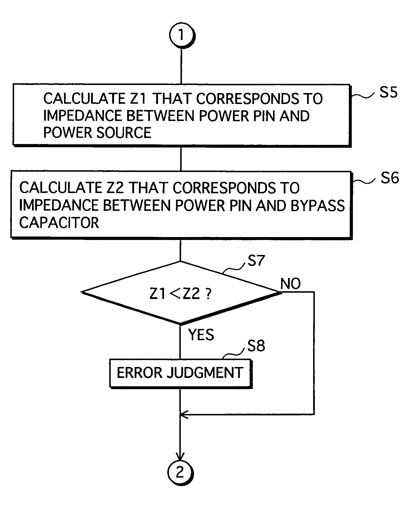
[0049]The layout check system of the present embodiment has the following features. In order to check-whether a PCB layout defined by created layout data will enable the bypass capacitors positioned on the PCB to function effectively, the layout check system first calculates a value Z1 that corresponds to the impedance between a power pin of a high-speed IC on the PCB and the power source, and a value Z2 that corresponds to the impedance between the power pin and a bypass capacitor. The layout check system then compares the calculate values, and when Z1 is less than Z2, judges that an error exists, and outputs error information.

Structure

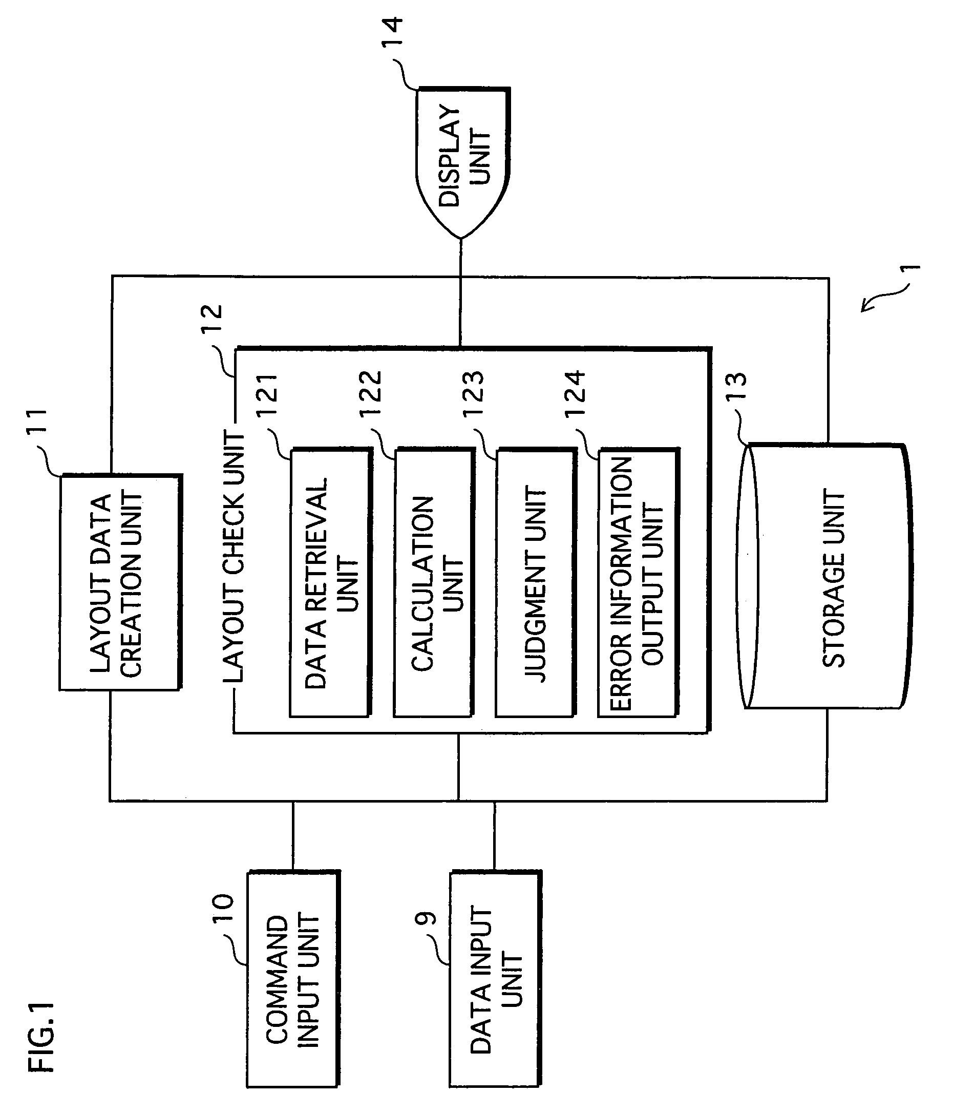
[0050]FIG. 1 shows the functional structure of the layout check system of the first embodiment.

[0051]The layout check system 1 is composed of functional units including a data input unit 9, a...

second embodiment

Overview

[0150]The layout check system of the second embodiment is identical to the layout check system 1 described in the first embodiment except for additional functions in the layout check unit 12.

[0151]The additional functions are a function of judging whether a power pattern to which a power pin of a high-speed IC is connected is a power plane called a “power island”, and a function of analyzing whether wiring exists between the power island and the main power plane (a plane that is directly connected to the power source) that is connected without a bypass capacitor.

[0152]A conventional check system does not check whether a PCB layout having a power island is a layout that allows a bypass capacitor positioned near the power island to control parasitic noise from the high-speed IC connected to the power island to function effectively.

[0153]The layout check system of the second embodiment is characterized in performing the following error judgments using the additional functions.

[...


PUM


Abstract

A layout check system checks whether a layout of a power source, a component including a power pin, and a bypass capacitor on a PCB and defined by layout data created using a CAD system allows the bypass capacitor to function effectively. A storage unit stores the layout data that includes information used as a basis to calculate a first value corresponding to impedance between the power pin and the power source and a second value corresponding to impedance between the power pin and the bypass capacitor. A calculation unit calculates the first value and the second value with use of the information. A judgment unit judges whether the layout allows the bypass capacitor to function effectively, by comparing the first value with the second value. When a result of the judgment is negative, an output unit outputs error information.

Description

BACKGROUND OF THE INVENTION[0001](1) Field of the Invention[0002]The present invention relates to a CAD (computer aided design) technique used in layout design of a printed circuit board (hereinafter called a “PCB”), and in particular to a technique for checking whether the layout of a PCB defined according to layout data created using a CAD system will enable bypass capacitors positioned on the PCB to function effectively.[0003](2) Description of the Related Art[0004]In recent years, high performance and digitalization of electronic devices has lead to the use of high-speed digital ICs (hereinafter called “high-speed IC(s)”) as main structural components of such electrical devices.[0005]A high-speed IC performs high-speed switching operations which cause high frequency fluctuations in the power source voltage and parasitic noise emission. For this reason, bypass capacitors are generally placed on the PCB on which a high-speed IC is mounted, positioned near the power pins of the hig...

Claims


Application Information

Patent Timeline
Patent Type & Authority Patents(United States)
IPC IPC(8): G06F17/50H05K1/02H05K3/00
CPCG06F17/5036G06F17/5081H05K1/0231H05K3/0005G06F30/367G06F30/398
Inventor TANIMOTO, SHINICHIMIMURA, SYOICHI
Owner PANASONIC CORP
Why Eureka
Try Eureka