Atomic layer deposition of interpoly oxides in a non-volatile memory device

a non-volatile memory and interpoly oxide technology, applied in the field of integrated circuits, to achieve the effect of reducing the number of defects

Inactive Publication Date: 2006-10-17
PROMOS TECH INC
View PDF16 Cites 70 Cited by
  • Summary
  • Abstract
  • Description
  • Claims
  • Application Information

AI Technical Summary

Benefits of technology

[0007]In some embodiments of the present invention, the silicon nitride layer of the ONO is substituted with a high-k dielectric layer formed by a deposition technique known as atomic layer deposition (ALD).(“High-k” refers to materials having a dielectric constant greater than about 4). Using ALD, single monolayers of the high-k material can be formed at a time, resulting in a nearly perfect crystal structure with fewer crystal defects or pin holes. Reducing the number of defects reduces the number of defect states, which allow undesired electron transport across the oxide barrier. Therefore the leakage current is minimized, while the dielectric constant remains higher than that of silicon dioxide by a factor of 2–6 times. Aspects of the invention include the method for forming the atomic monolayers, and their inclusion in an interpoly stack of a flash memory cell.

Problems solved by technology

However, the occurrence of high tunneling current through such thin layers of SiO2 requires that alternative materials be considered.

Method used


Image

  • Atomic layer deposition of interpoly oxides in a non-volatile memory device
  • Atomic layer deposition of interpoly oxides in a non-volatile memory device
  • Atomic layer deposition of interpoly oxides in a non-volatile memory device

Examples


Embodiment Construction

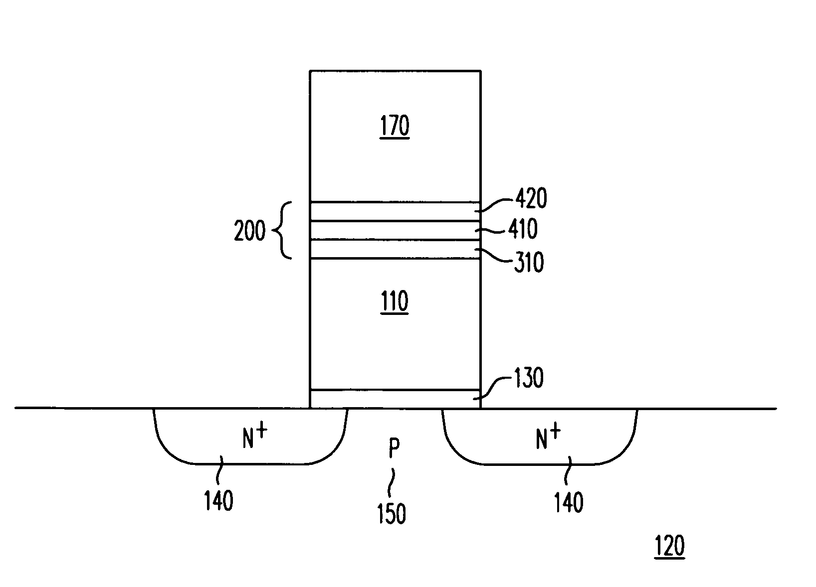
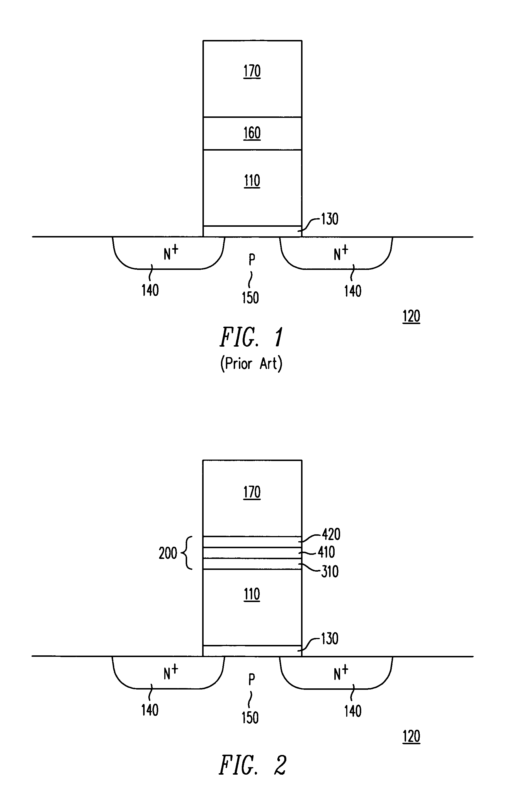
[0015]FIG. 2 illustrates a cross section of a nonvolatile memory cell at an intermediate stage of fabrication. In the illustrative embodiment being described, substrate 120 is a suitably doped (e.g. P-doped) monocrystalline silicon substrate; appropriate wells (not shown) have been formed in the substrate, as described in U.S. Pat. No. 6,355,524 entitled “Nonvolatile Memory Structures and Fabrication Methods”, filed Aug. 15, 2000 by H. T. Tuan et al., incorporated herein by reference. Other types of substrates, including non-silicon substrates, can also be used. The invention is not limited by any particular wells or doping types.

[0016]Source / drain regions 140 are formed by doping. Additional layers (not shown) may be formed to provide select gates, erase gates, or other features. See the aforementioned U.S. Pat. No. 6,355,524 B1 for an exemplary memory fabrication process that can be modified to incorporate the atomic-layer deposition oxide described above.

[0017]Semiconductor subst...


PUM


Abstract

Aluminum oxide is deposited by atomic layer deposition to form a high-k dielectric for the interpoly dielectric layer of a non-volatile memory device. The increased capacitive coupling can allow a thicker oxide layer to be used between the floating gate and the control gate, resulting in improved reliability and longer lifetime of the memory cells fabricated according to this invention.

Description

BACKGROUND OF THE INVENTION[0001]The present invention relates to integrated circuits, and more particularly to nonvolatile integrated memories.[0002]FIG. 1 shows a cross section of a stacked gate nonvolatile memory cell such as used in flash and non-flash electrically erasable programmable read only memories (EEPROM). Conductive floating gate 110, made of doped polysilicon, overlies monocrystalline silicon substrate 120. Silicon dioxide 130 insulates the floating gate from the substrate. N type source / drain regions 140 in substrate 120 are separated by[0003]type channel region 150. Channel region 150 is directly below the floating gate. Dielectric 160 separates the floating gate from control gate 170 made of doped polysilicon.[0004]The memory cell is read by applying a voltage between the regions 140, applying a voltage between one of the regions 140 and control gate 170, and detecting a current through the other one of the regions 140. The memory cell is written (programmed or era...

Claims


Application Information

Patent Timeline
Patent Type & Authority Patents(United States)
IPC IPC(8): H01L21/8238H01L21/28H01L21/316H01L29/51
CPCH01L21/02164H01L21/02178H01L21/022H01L21/02211H01L21/02271H01L29/511H01L21/02307H01L21/28273H01L21/3162H01L21/0228H01L21/28211H01L21/31683H01L29/40114
Inventor JANG, CHUCKDONG, ZHONGCHAN, VEI-HANCHEN, CHING-HWA
Owner PROMOS TECH INC
Why Eureka
Try Eureka