Stud-cone bump for probe tips used in known good die carriers

a probe tip and probe technology, applied in the field of known good die (kgd) carrier membrane, can solve the problems of limited use of conductive polymers that are screened upon the ceramic membrane, and limited use of plated bumps in the polymer membrane, so as to achieve greater ease of manufacture and reduce the production cost of the carrier membrane

Inactive Publication Date: 2006-10-17
TEXAS INSTR INC
View PDF6 Cites 1 Cited by
  • Summary
  • Abstract
  • Description
  • Claims
  • Application Information

AI Technical Summary

Benefits of technology

[0008]Advantages of the above described improvement are lower carrier membrane production costs relative to the prior art and greater ease of manufacture.

Problems solved by technology

At present, the known good die carrier industry is limited by the pad pitch and number of bumps that can be placed economically upon a single temporary test carrier used to manufacture KGD.
It has been demonstrated that the use of a polymer membrane with plated bumps is a technology that could not be easily developed.
The use of a conductive polymer that is screened upon the ceramic membrane is limited by the pitch constraints of the screening techniques which are pushed to the maximum at about 4 mils.
This is insufficient to support the newer generation of semiconductor devices.
A further problem encountered is the cost associated with the procuring of membranes used to route the signals in the test carriers.
The cost of fabricating such membranes is presently not economically viable.

Method used


Image

  • Stud-cone bump for probe tips used in known good die carriers
  • Stud-cone bump for probe tips used in known good die carriers
  • Stud-cone bump for probe tips used in known good die carriers

Examples


Embodiment Construction

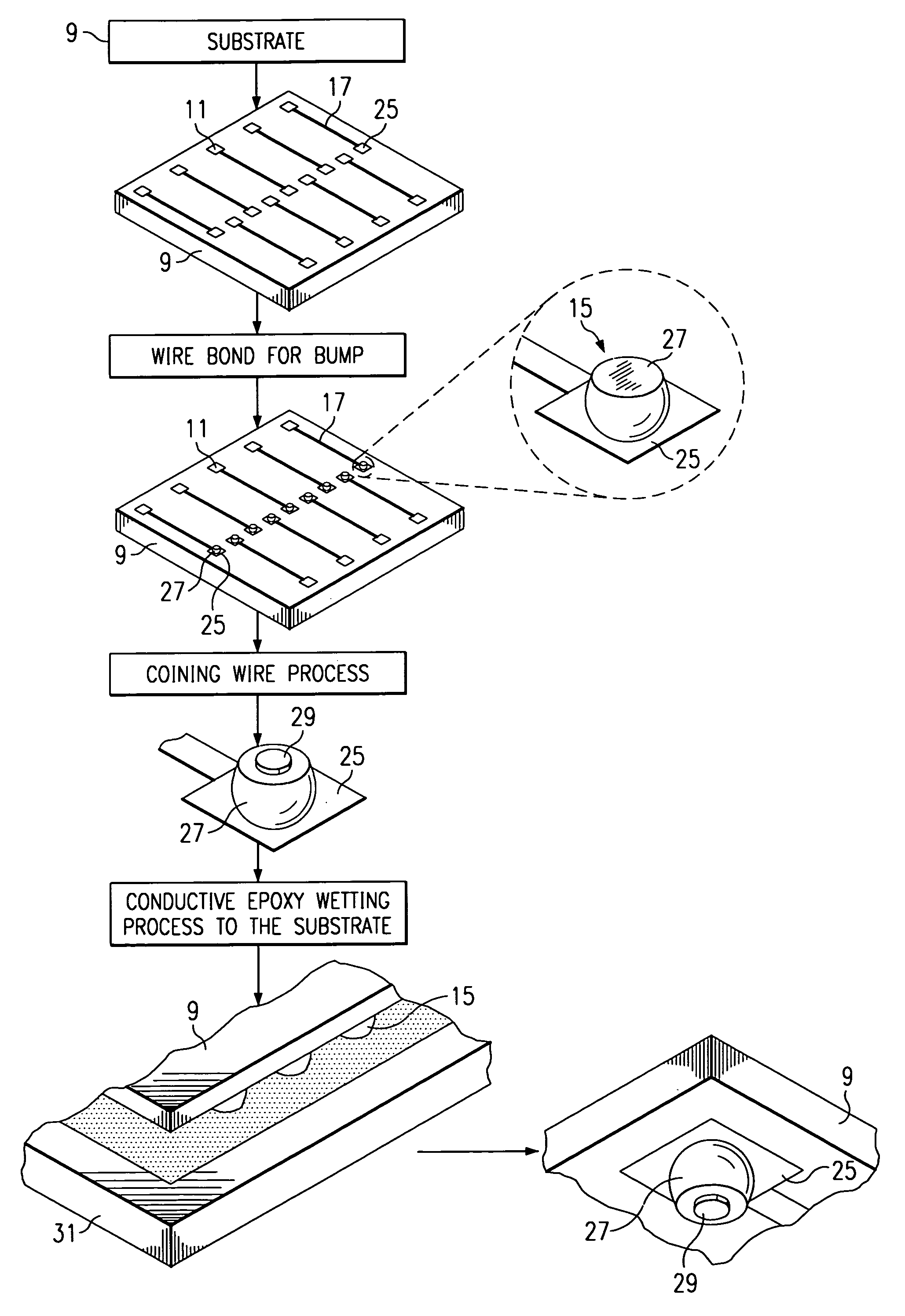
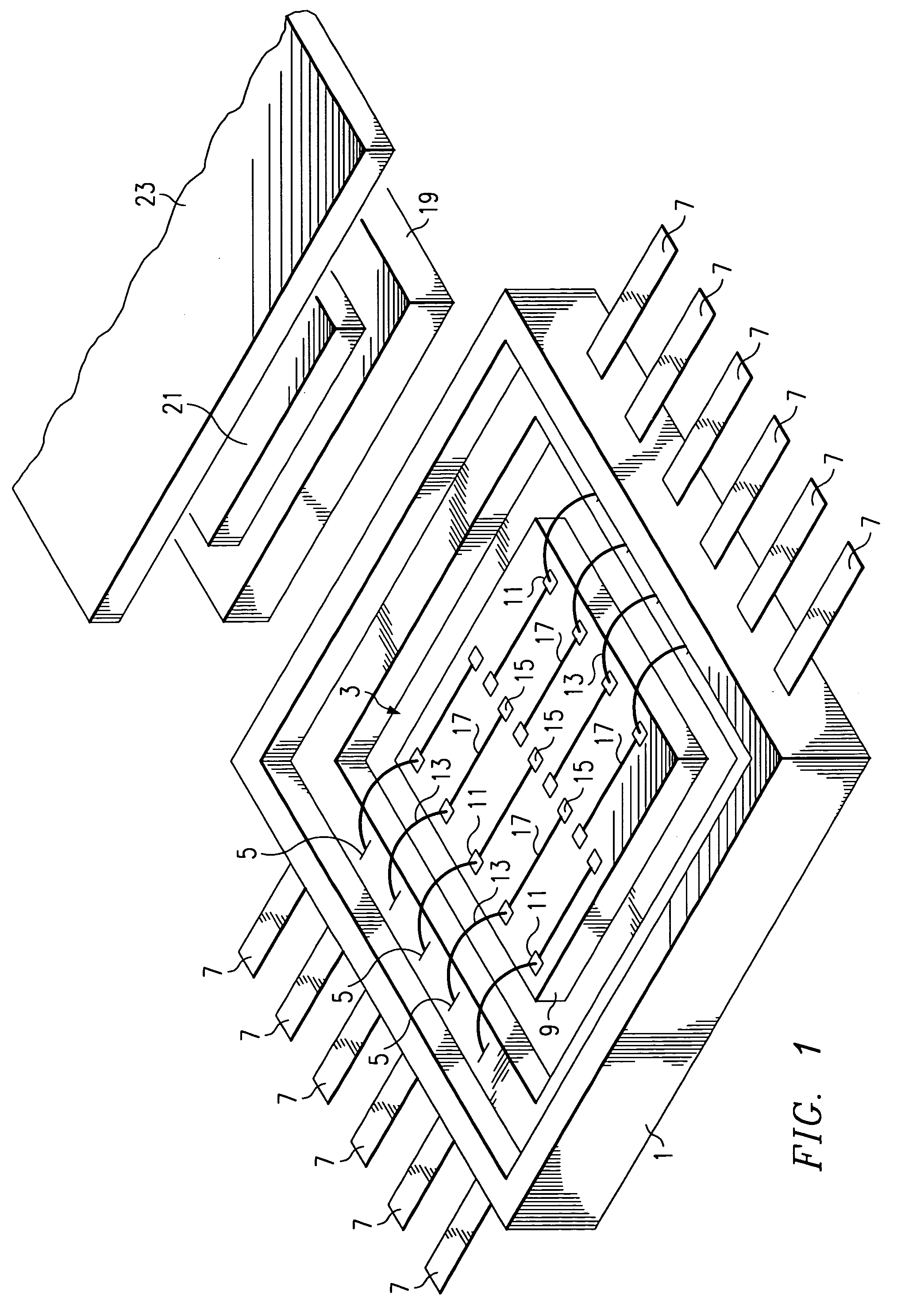
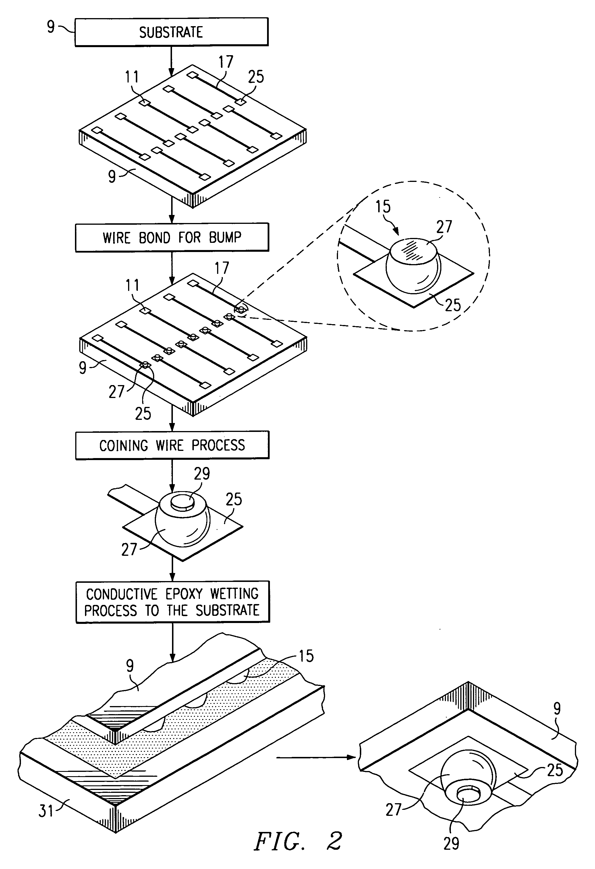
[0013]Referring to FIG. 1, there is shown a package which includes a header or carrier 1 having a cavity 3 with a plurality of terminals 5 disposed along the sidewalls of the cavity. The terminals 5 are coupled through an interconnect which extends through the wall of the header 1 to external leads 7 of the type shown in the above noted copending applications. A membrane 9, preferably of ceramic or silicon, is disposed on the floor of the cavity 3, the membrane having bond pads 11 thereon which are coupled by wires 13 to the terminals 5. The membrane 9 also includes thereon a plurality of stud bumps 15 with interconnect 17 connecting the stud bumps to the bond pads 11. A semiconductor die 19 having bond pads (not shown) on the underside thereof is disposed within the cavity 3 and over the membrane 9 so that the bond pads on the semiconductor die contact the studs 15 as will be explained in greater detail hereinbelow. A compliant material 21 is disposed in the cavity and over the die...


PUM

PropertyMeasurementUnit
thicknessaaaaaaaaaa
thicknessaaaaaaaaaa
thicknessaaaaaaaaaa

Abstract

A method of forming a membrane for use in conjunction with a semiconductor carrier and the membrane which includes an electrically insulating substrate and an interconnect pattern formed on the substrate. A stud is coupled to the interconnect pattern over the substrate by forming a gold ball, preferably by gold ball bonding techniques, and coating a portion of the gold ball with a compliant material, preferably an epoxy resin. The coating is filled with a material having sufficient hardness to be capable of penetrating the oxide film on the contact pads of semiconductor devices. The flakes are preferably silver or silver-based.

Description

CROSS REFERENCE TO RELATED APPLICATIONS[0001]This application is a division of Ser. No. 09 / 431,730, filed Nov. 1, 1999 now U.S. Pat. No. 6,376,352 which claims priority based upon provisional application Ser. No. 60 / 107,230, filed Nov. 5, 1998 and is related to Ser. No. 09 / 164,580, filed Oct. 1, 1998, the contents of which are incorporated herein by reference.FIELD OF THE INVENTION[0002]This invention relates to a known good die (KGD) carrier membrane and to a method of fabricating the membrane.BRIEF DESCRIPTION OF THE PRIOR ART[0003]At present, the known good die carrier industry is limited by the pad pitch and number of bumps that can be placed economically upon a single temporary test carrier used to manufacture KGD. A great deal of development work has been performed on this problem. It has been demonstrated that the use of a polymer membrane with plated bumps is a technology that could not be easily developed. The use of a conductive polymer that is screened upon the ceramic me...

Claims


Application Information

Patent Timeline
Patent Type & Authority Patents(United States)
IPC IPC(8): H01L23/52H01L23/48G01R1/04H01L21/48
CPCG01R1/0466H01L21/4853H01L2224/16H01L2224/48091H01L2224/48472H01L2224/73253H01L2924/01079H01L2924/15153H01L2924/15165H01L2924/16195H01L2924/19107H01L2924/00014H01L2224/48227H01L2924/00H01L2224/16145H01L2224/05568H01L2224/05573H01L2224/05599
Inventor ARNOLD, RICHARD W.BEARDAIN, WELDONWILSON, LESTER L.FORSTER, JAMES A.
Owner TEXAS INSTR INC
Why Eureka
Try Eureka