Method for Raman imaging of semiconductor materials

a semiconductor material and imaging method technology, applied in the field of raman imaging of semiconductor materials, can solve the problems of aotfs having distinct limitations, degrading imaging performance, and lack of tunable filters, and achieve high spatial and spectroscopic resolution and rapid characterization of semiconductor materials

Inactive Publication Date: 2006-10-17
CHEMIMAGE TECH
View PDF6 Cites 8 Cited by
  • Summary
  • Abstract
  • Description
  • Claims
  • Application Information

AI Technical Summary

Benefits of technology

[0009]It is an object of the invention to produce an apparatus, a method, and a system for r

Problems solved by technology

Prior to the introduction of LCTFs, a key limitation of tunable filters that had handicapped Raman microscopy had been the lack of the availability of tunable filters that simultaneously provided narrow spectral bandpass, broad free spectral range and high image quality.
For example, AOTF Raman imaging systems provide high throughput and broad spectral coverage, but AOTFs have distinct limitations.
AOTFs suffer from broad spectral bandpass, and ima

Method used


Image

  • Method for Raman imaging of semiconductor materials
  • Method for Raman imaging of semiconductor materials
  • Method for Raman imaging of semiconductor materials

Examples


Embodiment Construction

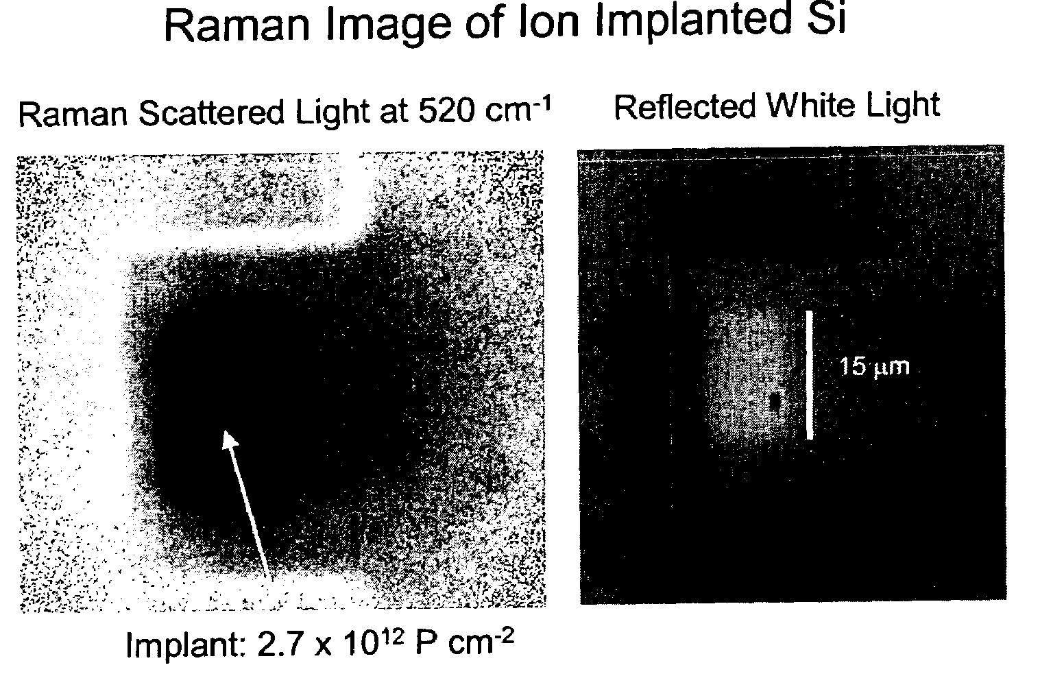
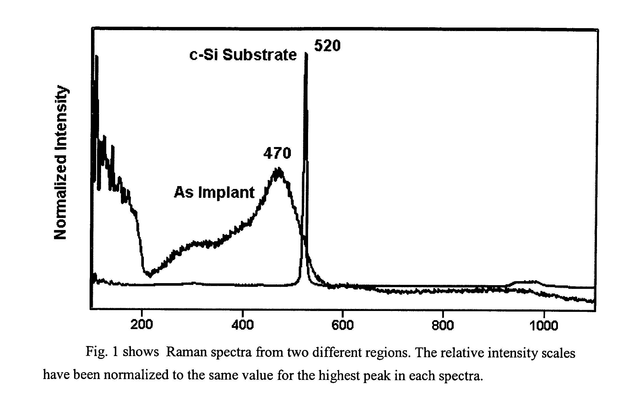
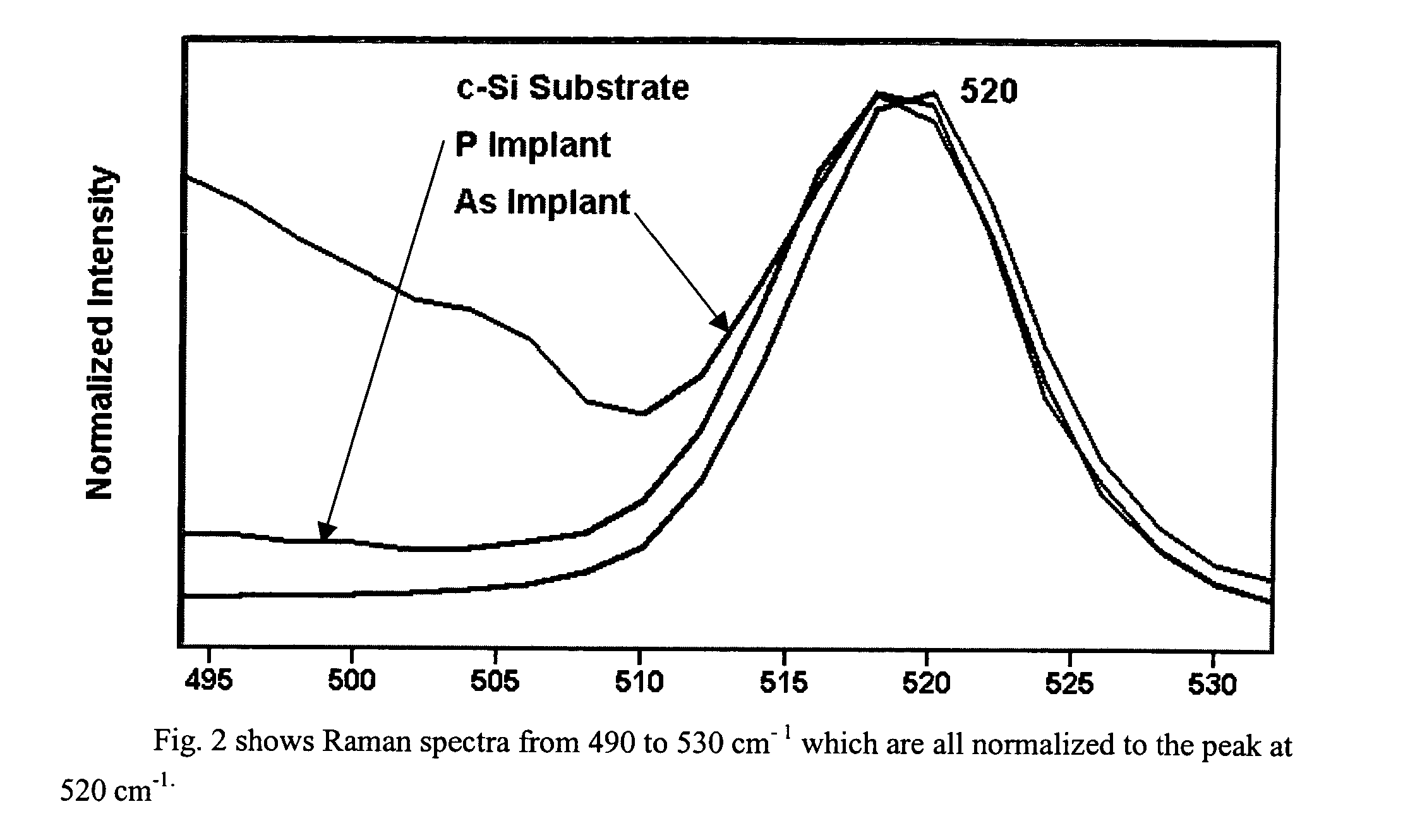
[0022]The inventors have realized that prior art imaging techniques were deficient in that the incident light was not reproducible enough over time to produces high enough quality images for materials characterization. In particular, inventors have realized that the prior art has no mechanism to record a comparison Raman signal simultaneously in the same image with the Raman signal from regions of interest. The present invention solves this previously unrecognized problem.

[0023]John Evans described a ‘split-element’ design that addresses the inefficiency of the Lyot design filters. The ‘split-element’ design cuts the number of polarizers in half, plus one, reducing the absorbance of light due to the polarizers. In addition, the λ / 2 waveplates are eliminated providing enhanced optical throughput. This yields an improved filter transmission ranging from 1.55–3.1 times that of the Lyot filter.

[0024]Imaging spectrometers include Fabry Perot angle rotated or cavity tuned liquid crystal (...


PUM


Abstract

An ion implanted semiconductor surface is illuminated with a flood illumination of monochromatic radiation, and an image of the surface is taken using light which has been Raman scattered. The illumination and imaging system are calibrated by flood illuminating a uniformly Raman scattering surface.

Description

CROSS REFERENCE TO RELATED APPLICATIONS[0001]This application is a continuation-in-part (CIP): of U.S. Non-Provisional application Ser. No. 09 / 619,371 filed Jul. 19, 2000 now U.S. Pat. No. 6,788,860 which claims benefit pursuant to 35 U.S.C. § 119(e) of U.S. Provisional Application 60 / 144,518 filed Jul. 19, 1999; of U.S. Non-Provisional application Ser. No. 09 / 976,391 filed Oct. 12, 2001 now U.S. Pat. No. 6,734,962 which claims benefit pursuant to 35 U.S.C. § 119(e) of U.S. Provisional Application 60 / 239,969 filed Oct. 13, 2000; and of U.S. Non-Provisional application Ser. No. 09 / 800,953 filed Mar. 7, 2001 now U.S. Pat. No. 6,717,668 which claims benefit pursuant to 35 U.S.C. § 119(e) of U.S. Provisional Application 60 / 187,560 filed Mar. 7, 2000. This application also claims benefit pursuant to 35 U.S.C. § 119(e) of U.S. Provisional Application 60 / 422,604 filed Oct. 31, 2002. All of the above applications are incorporated herein by reference in their entirety including incorporated ...

Claims


Application Information

Patent Timeline
IPC IPC(8): G01J3/44G01N21/00C08K9/02G01B11/25G01J3/28G01J3/447G01N21/35G01N21/65G02B6/32G02B21/00G02B21/06G02B21/36G06T5/50G06V40/13
CPCC08K9/02G01B11/2545G01J3/2823G01J3/44G01J3/447G01N21/65G02B21/00G02B21/06G02B21/365G06K9/00013G06T5/50G01N21/3563C08K2201/014G02B6/32G06V40/13
Inventor TUSCHEL, DAVIDTREADO, PATRICK J.DEMUTH, JOSEPH E.
Owner CHEMIMAGE TECH
Why Eureka
Try Eureka