Photoinduced charge-transfer materials for nonlinear optical applications

a charge-transfer material and nonlinear optical technology, applied in the field of nonlinear optical materials, can solve the problems of insufficient comparison of relative merits of different materials, inability to achieve maximum diffraction efficiency or response time, and difficulty in making multi-layers having arbitrary thicknesses, etc., and achieve the effect of enhancing the nonlinear optical properties of the nonlinear optical material

Inactive Publication Date: 2006-10-24
LOS ALAMOS NATIONAL SECURITY
View PDF16 Cites 19 Cited by
  • Summary
  • Abstract
  • Description
  • Claims
  • Application Information

AI Technical Summary

Benefits of technology

[0016]To achieve the foregoing and other objects, and in accordance with the purposes of the present invention, as embodied and broadly described herein, the method for generating materials which exhibit photoinduced charge transfer having a controlled direction hereof may include the steps of: depositing a donor layer onto a substrate, depositing a nonlinear optical material onto the donor layer, and depositing an acceptor layer onto the nonlinear optical material, whereby photoinduced charge transfer is achieved between the donor layer and the acceptor layer, thereby enhancing the nonlinear optical properties of the nonlinear optical material.

Problems solved by technology

However, simply comparing the maximum diffraction efficiency or the response time for different materials does not allow an adequate comparison of their relative merits, since rapid data processing requires having both a large response and a rapid recording rate.
Although materials having high thermal and chemical stability have been generated using these procedures, it has proven difficult to make multilayers having arbitrary thickness.
Additionally, materials, which incorporate photoinduced CT effects, have not yet been produced.
However, materials which incorporate photoinduced CT effects have not yet been produced by either covalent or ionic self-assembly methods.

Method used


Image

  • Photoinduced charge-transfer materials for nonlinear optical applications
  • Photoinduced charge-transfer materials for nonlinear optical applications
  • Photoinduced charge-transfer materials for nonlinear optical applications

Examples


example

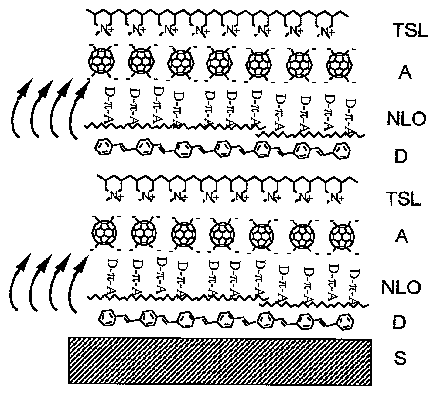
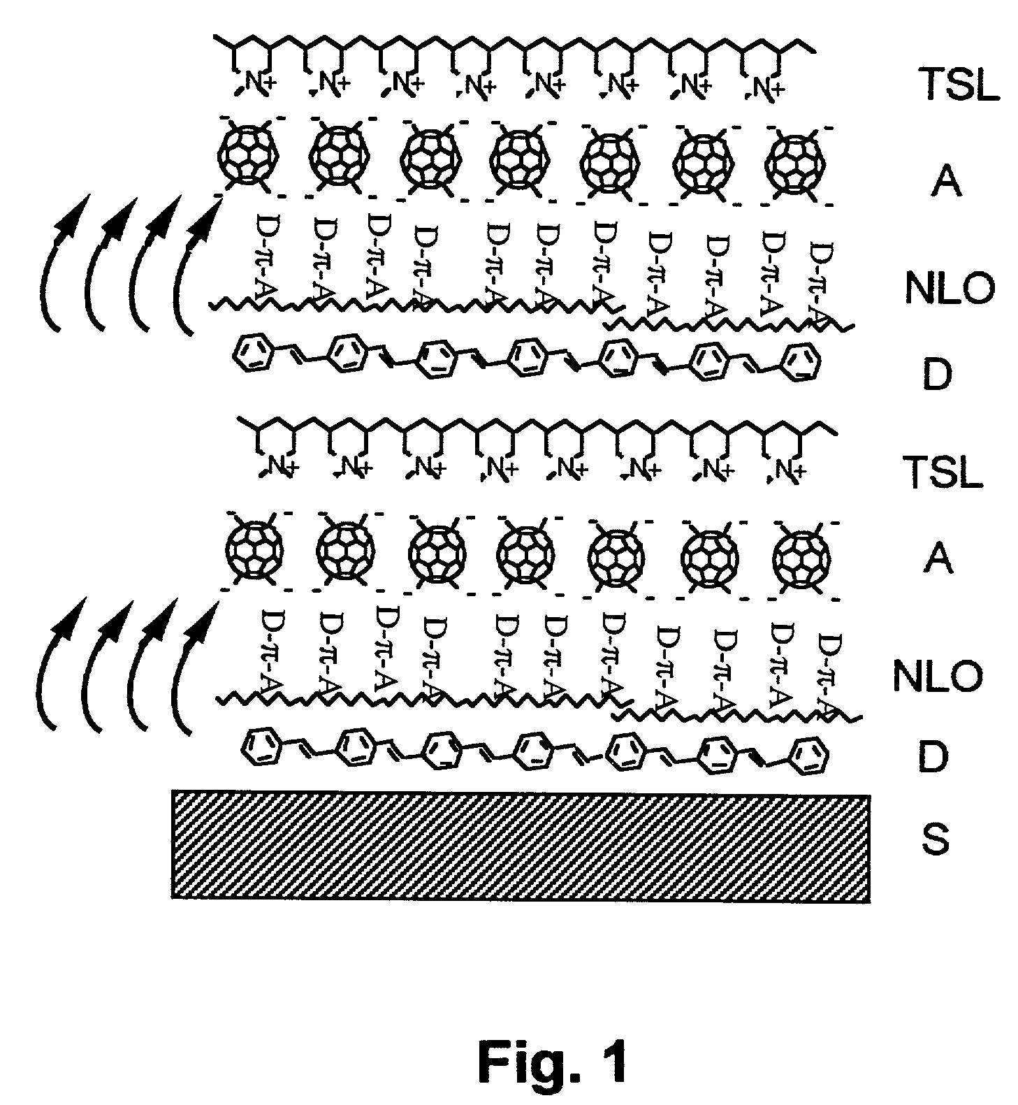
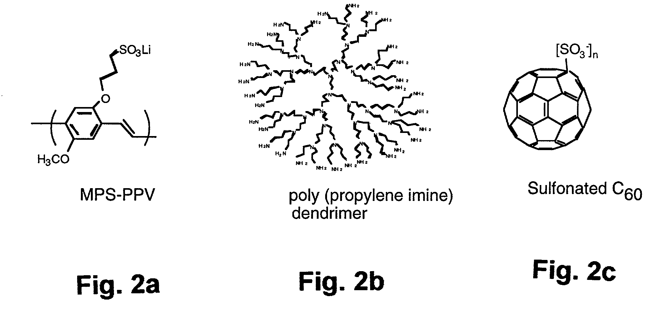
[0035]The anionic conjugated polymer poly(2,5 methyl-propyloxy sulfonate phenylene vinylene) (MPS-PPV) was synthesized according to well-known synthetic procedures. Cationic and anionic transparent binder compounds, including poly(propylene-imine) dendrimers (generation 3.0), poly(styrene sulfonate) (PSS) and PEI were purchased from Aldrich Chemical Co. and used without further purification. De-ionized water (DI) having >18MΩ resistivity from a Nanopore still was used for all aqueous solutions and rinses. The glass slides were cleaned by first placing them in an H2O2 / H2SO4 (30% / 70%) solution mixture at 80° C. for one hour and then sonicating them in 200 ml of de-ionized water for 30 min. These substrates were later rinsed with pure ethanol to produce hydrophilic surfaces. Concentrations of all polycation and polyanion aqueous solutions were in the range of 10−3 M. Self-assembled multilayer films were made by first immersing the substrate into the polycation solution and then in the ...


PUM


Abstract

A method using polyelectrolyte self-assembly for preparing multi-layered organic molecular materials having individual layers which exhibit ultrafast electron and / or energy transfer in a controlled direction occurring over the entire structure. Using a high molecular weight, water-soluble, anionic form of poly-phenylene vinylene, self-assembled films can be formed which show high photoluminescence quantum efficiency (QE). The highest emission QE is achieved using poly(propylene-imine) (PPI) dendrimers as cationic binders. Self-quenching of the luminescence is observed as the solid polymer film thickness is increased and can be reversed by inserting additional spacer layers of transparent polyelectrolytes between each active conjugated layer, such that the QE grows with thickness. A red shift of the luminescence is also observed as additional PPV layers are added. This effect persists as self-quenching is eliminated. Charge transfer superlattices can be formed by additionally incorporating C60 acceptor layers.

Description

[0001]This invention was made with government support under Contract No. W-7405-ENG-36 awarded by the U.S. Department of Energy to The Regents of The University of California. The government has certain rights in the invention.FIELD OF THE INVENTION[0002]The present invention relates generally to nonlinear optical materials and, more particularly, to the preparation of thin films of layered supramolecular materials having individual molecular layers which exhibit ultrafast electron and / or energy transfer in a chosen direction.BACKGROUND OF THE INVENTION[0003]Photoinduced charge and energy transfer in biological molecules form the basis for photosynthesis and vision. The initial absorption and electron transfer steps take place on femtosecond (fs, (10−15 s) to picosecond (10−12 s) timescales, and the active molecules are usually linear chain or cyclic ring systems with extended networks of π-orbitals, leading to electron delocalization along the entire molecule, strong optical absorp...

Claims


Application Information

Patent Timeline
Patent Type & Authority Patents(United States)
IPC IPC(8): B05D5/06
CPCB82Y20/00G02F1/3618
Inventor MCBRANCH, DUNCAN W.
Owner LOS ALAMOS NATIONAL SECURITY
Why Eureka
Try Eureka